

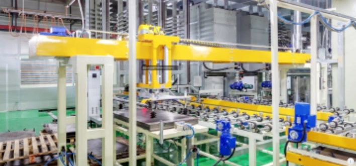
 NextPCB Capabilities
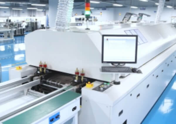
 PCB Assembly
 Layer Buildup
 SMD-Stencils
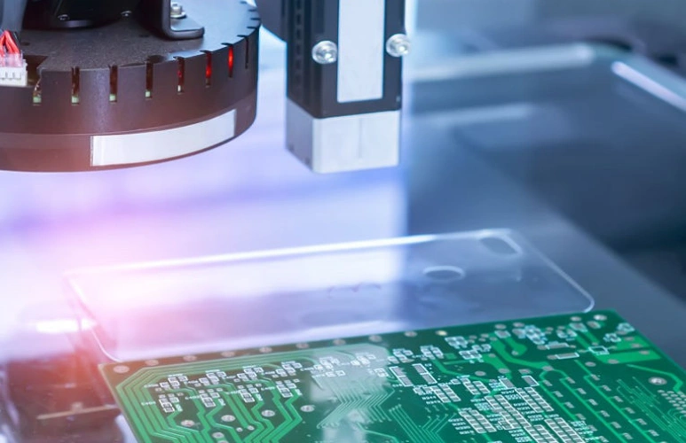
 PCB Design-Aid & Layout
 Mechanics
 Surface
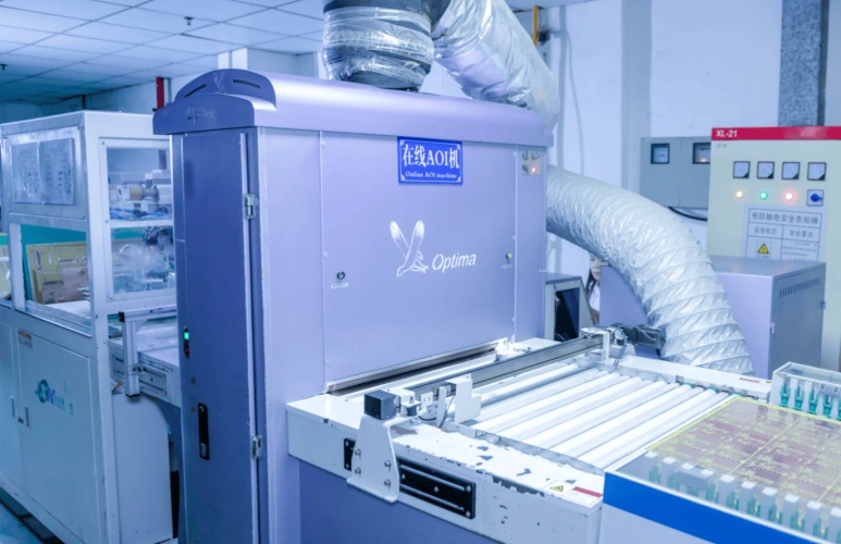
 Quality
 Drills & Throughplating
 Factory & Certificate


Printed circuit boards (PCBs) are the fundamental building blocks of almost all modern electronics, from consumer gadgets to mission-critical aerospace systems. The journey from a digital circuit design to a tangible, functioning electronic device is a complex, multi-stage process that demands precision, expertise, and a deep understanding of interconnected disciplines. This comprehensive guide serves as a pillar of knowledge for anyone involved in the electronics lifecycle, from design engineers to procurement managers and quality assurance professionals. It navigates the complete PCB manufacturing journey, covering everything from initial design considerations and bare board fabrication to component assembly, rigorous testing, and final delivery. By exploring the key processes, industry standards, and best practices, this guide provides a roadmap to ensure not only the functionality of a product but also its reliability, compliance, and cost-effectiveness.
Table of Content:
- 1. Concepts and Scope: The Distinction Between PCB Manufacturing and Fabrication
- 2. Design Preparation and Manufacturability (DFx): Ensuring Quality from the Design Source
- 3. Bare Board Fabrication Process and Quality Considerations
- 4. Assembly Processes (SMT/THT/Reflow/Selective Soldering) and Component Assurance
- 5. Testing and Inspection: The Quality Defense Line for Bare Boards and PCBA
- 6. Cleanliness and Reliability: No-Clean and Ionic Contamination Control
- 7. Protection and Post-Processing: Coating, Encapsulation, and Rework
- 8. Quality Management Systems and Industry Certifications: The Cornerstone of Credibility and Compliance
- 9. Supply Chain and Incoming Material Control: BOM Robustness and Traceability
- 10. Cost and Lead Time Engineering: Influencing Factors and Quoting Logic
- 11. Sustainability and Compliance Communication: ISO 14001, Environment, and Occupational Health
- 12. Glossary and Further Resources
I. Concepts and Scope: The Distinction Between PCB Manufacturing and Fabrication
In the electronics manufacturing industry, the terms "PCB Manufacturing" and "PCB Fabrication" are often used interchangeably, but they have fundamental differences in their technical scope and process. Clarifying the boundaries of these two concepts is essential for understanding the entire product lifecycle.
1. What is PCB Manufacturing?
In its broad sense, "PCB Manufacturing" is an end-to-end, full-value-chain integration process designed to transform circuit design files into a fully functional electronic product. This process is not limited to the production of the bare board itself; it is a comprehensive chain that includes multiple key services.
Broad manufacturing first encompasses bare board fabrication, which involves a series of chemical and physical processes to turn copper-clad laminates into multi-layer or single-layer circuit boards with predetermined circuit patterns, drilled holes, and structures. In addition to this, it also includes Bill of Materials (BOM) procurement, component assembly (SMT/THT), various tests and inspections, board cleaning and protective coating, and the final packaging and delivery. Therefore, the final output of broad manufacturing is a functional electronic assembly (PCBA) that is ready for immediate use. For a seamless and efficient experience, consider a turnkey solution like NextPCB that handles both fabrication and assembly under one roof.
2. What is PCB Fabrication?
In contrast, the narrow term "PCB Fabrication" is a single, critical subset of the overall manufacturing process. It focuses on converting a designer's circuit layout files (typically Gerber files) into a physical bare board, which is a blank circuit board without any electronic components. The output of this process is usually used for visual inspection, performance verification, or as an input for a subsequent assembly service. Understanding this difference is crucial because it directly impacts a project's timeline, cost, and communication efficiency. If a designer only orders bare board fabrication services, they will receive a stack of circuit boards that do not contain any components and are not functional. If a working prototype or finished product is needed, one must order or select a broad manufacturing service, which includes the entire set of services, including assembly.
3. Turnkey PCB Services
The evolution of the industry also reflects this conceptual integration. In the past, bare board fabrication and component assembly were often provided by different suppliers, which led to multiple data handover points, complex logistics, and blurred lines of responsibility. For example, invisible manufacturing defects on a bare board might not be discovered until after assembly, resulting in expensive rework costs.
To solve these pain points, turnkey service providers like NextPCB have emerged on the market. This model integrates bare board fabrication and component assembly under one roof and uses proactive Design for Manufacturability (DFM) checks to ensure that design files can seamlessly adapt to subsequent production processes, thereby significantly reducing communication costs, logistics delays, and improving overall yield.
Establishing a rigorous quality context for the entire process is inseparable from the support of industry standards. In the bare board fabrication stage, IPC-6012 specifies the performance and qualification requirements for rigid printed boards, while IPC-A-600 provides a visual guide to the acceptance criteria for printed boards. In the component assembly stage, IPC-J-STD-001 details the material, method, and acceptance requirements for soldering, while IPC-A-610 serves as the most widely used "picture book," providing a common visual guide for the acceptability of electronic assemblies. Together, these standards form the foundation for quality management and communication in the broad PCB manufacturing process.
> Recommend reading: The Core of System Integration: Box Build Assembly in Electronics Manufacturing
II. Design Preparation and Manufacturability (DFx): Ensuring Quality from the Design Source
The success of a PCB design is not just about achieving circuit functionality; it's about ensuring from the start that it can be manufactured efficiently, at low cost, and with a high yield. This is the core of the Design for Manufacturability (DFx) philosophy. By front-loading the principles of Design for Manufacturability (DFM), Design for Assembly (DFA), and Design for Testability (DFT) into the design phase, many risks in later production can be avoided.
> Recommend reading: DFM, DFMA, DFA. Part 1. Kicad and Online Gerber Viewer
> Recommend reading: DFM, DFMA, DFA. Part 2. NextPCB's PC program
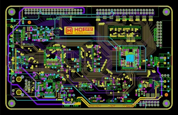
1. The Competition and Choice of Data Formats: Gerber vs. IPC-2581 vs. ODB++
In PCB manufacturing data transfer, the choice of file format directly affects the efficiency and accuracy of the entire supply chain.
-
Gerber X2: As an intelligent upgrade to the traditional RS-274X format, Gerber X2 adds key information such as layer stack-up definitions, pad and via attributes while maintaining backward compatibility. This improvement allows designers to include more manufacturing details in a single set of files. However, the main limitation of Gerber X2 is that it does not contain component information or the Bill of Materials (BOM), which means that to perform assembly and procurement, additional files such as PNP (Pick-and-Place) and BOM must be generated. This separate data transfer model increases data handover points and carries the risk of errors due to version mismatches or file loss. For teams that prefer a conservative upgrade or a segmented supply chain, this is a viable option. > How to Generate Gerbers from KiCad (Updated for KiCad 9)
-
IPC-2581 and ODB++: These two formats represent the future direction of data transfer—unification. They can integrate all the information required for bare board fabrication and component assembly, including copper layer images, stack-up information, netlists, BOM, placement coordinates, drill data, and manufacturing/assembly parameters, into a single, intelligent file. This "one-stop" data model greatly simplifies the data handover between designers and manufacturers, fundamentally eliminating errors caused by incomplete files or information mismatches. For turnkey service providers who seek seamless and efficient production, this is an ideal choice.
2. In-depth Analysis of Core DFM/DFT/DFA Principles
The three DfX principles are not independent; they interact to form a comprehensive quality assurance system for the entire PCB production lifecycle.
- Design for Manufacturability (DFM): The core of DFM is to ensure that the bare board layout meets the manufacturer's process capabilities, thereby achieving a high yield and low cost. This includes designing the board size and shape to maximize panel utilization, using a symmetrical layer stack-up to prevent board warping under thermal stress, and ensuring that trace widths and spacing meet the manufacturer's minimum tolerance requirements. Ignoring DFM can lead to the bare board being scrapped during the manufacturing process due to issues like insufficient annular rings for vias or copper traces being too close, resulting in high cost losses.
- Design for Assembly (DFA): DFA focuses on the placement and soldering process of components. Its principles require designers to ensure that component spacing, component-to-board edge distance and pad design all meet the requirements of automated placement machines, thereby avoiding in the pick-and-place and reflow soldering processes appears wrong bit, tin bridge or missing solder and other defects. For example, correct component polarity marking and consistent component orientation are key to improving the efficiency of automated assembly. > DFA in DFMA: Avoid Costly PCB Assembly Errors | NextPCB Case Studies
- Design for Testability (DFT): DFT is a proactive quality strategy. It requires designers to reserve test points, test windows, and board edges on the PCB so that electrical tests can be performed quickly and accurately after fabrication and assembly to rapidly diagnose and isolate faults. The lack of a DFT design may mean that even if a functional test (FCT) finds a problem, the specific defect cannot be quickly located, making the debugging and rework process time-consuming and labor-intensive, and possibly leading to the expensive board being scrapped.
3. Design Essentials and Quality Checklist
Translating the above principles into specific engineering practices can guide designers to avoid common risks:
- Stack-up and Materials: Using a symmetrical stack-up is a basic principle of DFM, as it can effectively balance the expansion differences of copper layers at high temperatures, preventing board warping during manufacturing and reflow soldering.
- Tolerances and Spacing: Designers must strictly follow the manufacturer's provided design rules for minimum trace width, spacing, drill size, and aspect ratio. For example, an insufficient annular ring for a via is the main cause of drill breakout and electrical opens.
- Test Point Design: The design of test point size, spacing, and location must meet the requirements of ICT or flying probe test fixtures. For example, test points usually need to have a certain minimum size, and there needs to be enough spacing between them to prevent probe shorts.
DFx is not just about technical details; it's a proactive risk management strategy that spans the entire product lifecycle. Design teams who invest effort in DFM, DFA, and DFT checks in the early stages can effectively avoid the costly consequences that may arise in later production. This embodies the core idea of "prevention is better than correction" in quality management systems. For example, a manufacturer with ISO 9001 certification will usually provide DFM feedback to help designers in the file sent to the production line before identifying and correcting potential problems, thereby avoiding re-fabrication and delays caused by design defects.
Get Fast Free DFM Feedback at NextPCB
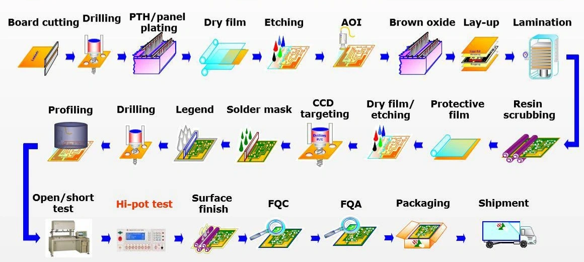
III. Bare Board Fabrication Process and Quality Considerations
Bare board fabrication is the key process that transforms design files into a physical circuit board. The process consists of a series of complex and precise steps, where quality control at each stage is crucial.
1. Detailed Core Processes
The complete bare board fabrication process includes the following key steps:
- a. Cutting and Inner Layer Imaging: First, an appropriate panel is cut from a large sheet of copper-clad laminate according to the design size. For multi-layer boards, the inner layer circuit pattern is transferred by photolithography, where a photoresist dry film is laminated onto the copper foil, then exposed with a laser or ultraviolet light to form a negative image of the circuit. Afterward, unnecessary copper foil is removed through chemical etching to reveal the final circuit traces and pad patterns.
- b. Lamination: The etched inner layers, prepreg (semi-cured bonding material), and copper foils are precisely pressed together under high temperature and pressure to form a solid multi-layer structure. The quality of this process directly affects the final board's mechanical stability.
- c. Drilling: A CNC drilling machine is used to precisely drill vias and through-holes in the board. For high-density interconnect (HDI) boards, microvias are created using laser drilling technology. The number, size, and location of the holes are important factors affecting cost and manufacturing difficulty.
- d. Chemical Plating and Electroplating: After drilling, a thin conductive copper layer is chemically deposited on the hole walls and board surface, followed by electroplating to increase the copper thickness to the design requirements. This step is critical for achieving electrical connections between different layers, and its quality directly determines the board's reliability.
- e. Solder Mask and Silkscreen: After electroplating and etching are complete, a layer of solder mask ink is applied to the board's surface. This not only protects the circuit but also prevents shorts during soldering. Afterward, silkscreen is printed on the solder mask layer to label component locations, polarities, company logos, and other information.
- f. Surface Finish: To protect exposed pads from oxidation and provide good solderability, a surface finish is applied. Common finishes include Hot Air Solder Leveling (HASL), Electroless Nickel Immersion Gold (ENIG), Electroless Nickel Electroless Palladium Immersion Gold (ENEPIG), and Organic Solderability Preservative (OSP). The cost of different surface finishes varies; for example, ENIG is usually more expensive than HASL.
- g. Profiling and Electrical Test (E-test): Finally, individual circuit boards on the production panel are separated by CNC routing or V-scoring. After this, all boards must undergo a 100% electrical test to ensure there are no open or short circuit problems. > Recommend reading: How to avoid shorts and opens in PCB Design using Design for Manufacture (DFM) tools?
2. IPC-6012 & IPC-A-600 Standard Application and Quality Points
IPC-6012 and IPC-A-600 are two indispensable standards in bare board quality control, as they specify requirements for PCBs from different perspectives.
- IPC-6012 (Performance and Qualification): This is a performance-based standard that focuses on specific performance indicators of bare boards in electrical, mechanical, and environmental aspects. It specifies hard metrics such as hole copper thickness, dielectric layer thickness, and solderability. For example, for high-reliability Class 3 products, the plated copper thickness in a via is usually required to be at least 1 mil (about 25 μm) to ensure long-term reliability.
- IPC-A-600 (Visual Acceptability): This is a visually-based inspection standard. It provides a basis for manufacturers and customers to judge whether bare board visual defects are acceptable through a large number of illustrations and descriptions. It covers all externally visible features such as pads, vias, traces, and solder mask.
Using these two standards together is a necessary strategy to ensure high quality. Relying solely on IPC-A-600 for visual inspection carries huge risks because some fatal internal defects, such as insufficient hole copper thickness or poor interlayer bonding, are invisible to the naked eye. These defects can directly lead to product failure under thermal stress or during long-term service.
Similarly, Conductive Anodic Filament (CAF), an internal electrochemical corrosion phenomenon in multi-layer boards, cannot be judged by appearance in its early stages but can cause a short circuit over time. Therefore, a truly high-quality manufacturer will not only ensure that the product's appearance is perfect according to IPC-A-600 but will also perform rigorous internal performance tests, such as cross-section analysis, according to IPC-6012 to fundamentally guarantee the product's long-term reliability.
The table below compares the different focuses of IPC-6012 and IPC-A-600 on several key quality indicators, showing their complementary relationship.
|
Metric |
IPC-A-600 Visual Standard |
IPC-6012 Performance Standard |
Common Defects |
Acceptability Level (e.g., Class 3) |
|
Hole Copper Thickness |
Checks for visible defects at the hole opening, such as copper voids or burrs |
Specifies minimum plated copper thickness inside the hole; e.g., Class 3 requires at least 1 mil |
Plating too thin, voids, cracks |
Must meet minimum thickness requirement, no voids, no cracks |
|
Checks the concentricity of the pad and drill hole with illustrations to judge for breakout |
Specifies minimum annular ring size; Class 3 requires 2 mil for external layers and 1 mil for internal layers |
Breakout or tangency caused by misaligned drilling |
No breakout allowed |
|
|
Checks if the solder mask dam between pads is complete and without defects |
Specifies minimum width to prevent soldering shorts |
Missing or excessively narrow solder mask dam |
Must meet minimum width requirement to ensure pad independence |
|
|
Conductive Anodic Filament (CAF) |
Cannot be judged by visual inspection, as it's an internal failure mechanism |
Focuses on material selection, drilling process, etc., to mitigate CAF risk |
Short circuit due to degradation of the resin/glass interface |
Must use CAF-resistant materials and have strict process control |
3. Managing PCB Quality with SPC & Capability Indices (Cp/Cpk)
SPC (Statistical Process Control) tracks critical PCB characteristics like plated thru-hole (PTH) copper thickness, trace width/spacing accuracy, controlled impedance, board thickness/flatness (warpage), surface finish thickness (e.g., ENIG, HASL), and solder mask thickness. Regular GR&R (Gauge Repeatability & Reproducibility) studies confirm measurement accuracy. Monitor production stability using Control Charts:
X-bar/R chartsfor measurable variables (e.g., thickness, impedance).p-charts / u-chartsfor defect percentages/rates (e.g., non-conforming boards).
Process Capability Analysis (Cp/Cpk) quantifies how well your process meets specifications:
- Cp = (USL – LSL) / (6σ)
- Measures process potential (Can the process possibly fit within tolerance?).
- Cpk = min[(USL - µ)/(3σ), (µ - LSL)/(3σ)]
- Measures actual performance (Is the process centered and within tolerance?).
- USL/LSL = Upper/Lower Specification Limit
- µ = Process Mean
- σ = Process Standard Deviation
Capability Targets:
- ≤ Class 2 (Standard): Cpk ≥ 1.33
- ≥ High-Reliability (Medical, Automotive, Aerospace): Cpk ≥ 1.67 (Unless customer specifies higher).
Correcting Low Cpk: If Cpk falls below target, investigate and retune key processes such as:
- Plating: Current density, bath agitation, chemical concentration/concentration control, immersion time.
- Imaging/Develop/Etch: Exposure, develop time, etchant concentration/parameters.
- Stack-up/Trace Models: Material selection, layer prepreg thickness during lamination, impedance calculation accuracy.
Output & Benefit: Generate monthly trend dashboards tracking Cp/Cpk for all key characteristics. Stabilized and capable processes dramatically reduce defects (test escapes discussed in Section V), lower costs, and ensure reliability for high-reliability electronics.
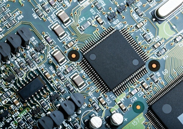
IV. Assembly Processes (SMT/THT/Reflow/Selective Soldering) and Component Assurance
PCB assembly is the process of combining a bare board with components to give it electrical functionality. This process primarily relies on Surface Mount Technology (SMT) and Through-Hole Technology (THT), and is subject to strict material and environmental controls.
> Recommend reading: PCB Assembly - The Most Comprehensive Guide | NextPCB
1. SMT and THT Process Flow
SMT (Surface Mount Technology):
SMT is the mainstream assembly technology today, popular because it can achieve high-density, small-sized component mounting. Its core process includes:
- Solder Paste Printing: Using a laser-cut stencil, solder paste is precisely printed onto the pads of the bare board.
- SPI (Solder Paste Inspection): A 3D inspection is performed immediately after solder paste printing to ensure the volume, shape, and position of the paste are fully compliant with design requirements. This pre-emptive inspection greatly improves the yield of subsequent reflow soldering and effectively prevents soldering defects caused by insufficient or excessive solder. > Recommend reading: SPI vs. I2C vs. UART: Differences Between These Communication Interfaces
- Pick-and-place: High-speed, high-precision pick-and-place machines use vacuum nozzles to pick up components from feeder tapes and accurately place them on the solder paste according to the coordinates and angle information in the PNP file.
- Reflow Soldering: The assembled PCB is conveyed into a reflow oven. Through a strictly controlled temperature curve (preheat, soak, reflow, cool), the solder paste melts to form a solid solder joint.
- AOI (Automated Optical Inspection): After reflow soldering, an AOI system uses high-resolution cameras to automatically check for component misalignment, reversed polarity, missing components, as well as surface defects like solder bridges and cold joints.
THT (Through-Hole Technology):
THT is a traditional assembly technology, primarily used for larger, heavier components or those requiring higher mechanical strength connections. The process includes:
- Component Insertion: Components are manually or machine-inserted into pre-drilled holes in the board.
- Wave Soldering or Selective Soldering: For through-hole components, wave soldering or selective soldering is typically used. Wave soldering passes the bottom of the PCBA over a wave of molten solder, completing the soldering of all through-holes at once. Selective soldering uses a precisely controlled nozzle to solder only specific areas, which is especially suitable for mixed-technology boards.
2. Material and Environment Control: J-STD-033 and ANSI/ESD S20.20
Product reliability depends not only on the assembly process but also on the strict control of incoming materials and the production environment.
-
Moisture Sensitive Devices (MSD) Control:
Many semiconductor components are sensitive to moisture. If a component absorbs too much moisture before reflow soldering, the moisture will vaporize and expand at high temperatures, causing the package to crack (known as the "popcorn effect"). To prevent this, the industry follows the IPC/JEDEC J-STD-033 standard, which specifies moisture-proof packaging (e.g., using moisture barrier bags and humidity indicator cards), dry baking, and strict management of their exposure time in the workshop.
-
Electrostatic Discharge (ESD) Protection:
Electrostatic discharge can cause permanent damage to sensitive components, and this damage is often undetectable through conventional testing, leading to unexpected product failures for the customer. ANSI/ESD S20.20 is a comprehensive electrostatic protection system standard that specifies a full set of requirements from anti-static workstations, wrist straps, anti-static flooring, and packaging bags to employee training, ensuring that components are effectively protected from static electricity throughout the entire process, from material reception to final product delivery.
V. Testing and Inspection: The Quality Defense Line for Bare Boards and PCBA
Testing is the last line of quality defense in PCB manufacturing, aiming to verify the product's functionality and reliability. The choice of testing method is not arbitrary but an engineering decision based on a comprehensive trade-off between product maturity, production volume, and budget.
> Recommend reading: PCB/PCBA Test Methods by Category
1. Bare Board Electrical Testing
Before PCB assembly, bare boards must undergo electrical testing to ensure there are no manufacturing defects such as open or short circuits.
- Flying Probe Test: This method uses multiple movable probes that, based on the netlist information in the design file, contact test points or pads one by one to detect open/short circuit issues. The advantage of flying probe testing is that it does not require expensive custom fixtures, making it very suitable for prototypes or small-batch, multi-variety production models because the test program can be easily modified when the design changes. However, its disadvantage is that the testing speed is relatively slow, making it unsuitable for large-scale mass production.
- Fixture Test: This method uses a customized "bed-of-nails" fixture where an array of probes corresponds one-to-one with all the test points on the board. During the test, the board is pressed onto the fixture, and all connection points are tested simultaneously, making it extremely fast. Although the manufacturing cost of a fixture is high, its extremely high test efficiency makes the unit cost very low in large-volume production.
2. Comprehensive PCBA Inspection Methods
PCBA testing is a multi-level system, and each method has its specific purpose and application scope.
- SPI (Solder Paste Inspection): As a preventive test, SPI is performed after solder paste printing and before component placement to ensure the volume, shape, and position of the solder paste are correct, thereby preventing reflow soldering defects.
- AOI (Automated Optical Inspection): AOI is performed after reflow soldering. It uses high-resolution cameras to visually compare the board against a standard "golden board" to check for component misalignment, polarity reversal, missing components, and surface defects of solder joints (such as solder bridges). It is fast and low-cost, but it cannot detect hidden solder joint issues under components like BGAs.
- AXI (Automated X-ray Inspection): AXI can "see through" to inspect hidden solder joints under packages like BGAs and QFNs, identifying empty holes, short circuits, and other internal defects. It offers the highest defect coverage, but the test speed is slow and the cost is high.
- ICT (In-Circuit Test): ICT uses a customized "bed-of-nails" fixture to perform a powered electrical performance test on each component of the PCBA (e.g., resistance, capacitance values) and check for opens and shorts. It can quickly and accurately locate almost all component-level manufacturing defects. ICT has extremely high fault diagnostic capability, but the fixture cost is high, so it is mainly used for mass production of mature products.
- FCT (Functional Test): FCT is the "final exam" for a PCBA. It simulates the final product's working environment to verify the overall function of the PCBA. It only gives a "pass" or "fail" result but does not provide specific fault diagnostic information. > Recommend reading: ICT vs FCT: PCBA Test Strategy
- Boundary Scan: This is a test technology based on the JTAG interface, mainly used to check the interconnects between high-density digital ICs. Its advantage is that it can test without physical contact, making it particularly suitable for complex circuits with dense pins and no test points.
The choice of PCBA testing strategy reflects a trade-off between production volume, product maturity, and cost.
For prototypes and small-batch production, since designs may be iterated frequently, an expensive ICT fixture is not cost-effective. Therefore, the combination of flying probe test + AOI + manual functional test is an ideal choice. The flying probe test can flexibly adapt to design changes and provide electrical diagnostics, AOI quickly checks for surface defects, and the manual test verifies core functionality.
When a product enters the mass production stage, the focus of testing shifts to efficiency and cost control. At this point, the golden combination of AOI + ICT + FCT becomes the industry standard. AOI and ICT form a powerful "manufacturing defect filter" that can quickly find and isolate most problems early in the production line, greatly reducing rework costs. Although ICT has a high initial investment, its extremely fast test speed significantly lowers the cost per board. FCT serves as the final check before shipment, ensuring all products have complete functionality.
|
Test Method |
Primary Purpose |
Applicable Scenario |
Pros & Cons |
|
SPI |
Checks solder paste print quality |
All SMT production lines |
Pros: Strong prevention, can detect issues early in production Cons: Solder paste only, cannot check components or solder joints |
|
AOI |
Inspects component position, polarity, and surface defects of solder joints |
Continuous quality control, especially suitable for SMT production lines |
Pros: Fast, low-cost, suitable for mass production Cons: Cannot detect hidden solder joints, limited coverage |
|
AXI |
Inspects hidden solder joints under BGA, QFN, and other packages |
Complex components, high-reliability products |
Pros: High accuracy, can detect internal defects Cons: Slower, high cost |
|
ICT |
Checks component electrical performance and for opens/shorts |
High-volume, mature products |
Pros: Strong diagnostic capability, fast, high coverage Cons: High fixture cost, not suitable for prototypes |
|
Flying Probe Test |
Checks for opens/shorts and basic electrical performance |
Prototypes, small-batch production |
Pros: No custom fixture needed, flexible with design changes Cons: Slow, not suitable for high-volume production |
|
FCT |
Verifies overall PCBA functionality |
All finished boards, as the final test before shipping |
Pros: Directly verifies product function, ensures customer experience Cons: Cannot diagnose specific faults, requires other tests |
|
Boundary Scan |
Checks digital IC interconnects |
High-density, complex digital circuits without test points |
Pros: No physical contact required, high test coverage Cons: Limited to digital ICs that support this technology |
3. Critical PCB testing KPIs
PCB testing KPIs like Net Coverage (tested nets/total nets), component/pad coverage, and DPPM (Defects Per Million) measure test thoroughness and product quality risk (escape rate). Your test strategy (sampling vs. 100%) must align with industry standards:
- Bare Board Testing: Target 100% coverage for opens/shorts testing (add insulation/hi-pot for critical apps). This is foundationally required.
- PCBA Test Strategy: Achieve >95% joint coverage with SPI (Solder Paste Inspection) + AOI (Automated Optical Inspection). Use X-ray for hidden joints (BGA/critical connections), choosing 100% or sampling based on risk. Prioritize boundary scan and FCT (Functional Circuit Testing) on critical signal paths.
Sampling vs. 100% by Industry:
- Automotive/Medical/Aerospace: 100% bare board + 100% AOI, 100% X-ray on critical joints, and comprehensive FCT (strictest).
- Industrial: 100% bare board, 100% AOI, X-ray sampling (high-frequency/targeted), and FCT sampling (tighten if DPPM increases).
- Consumer Electronics: 100% bare board, 100% AOI, risk-based X-ray sampling, and standard FCT sampling.
- Prototypes: Flying-probe test, 100% AOI, and focused functional checks.
Focus: Higher-risk industries demand 100% coverage for key tests (X-ray/FCT), while sampling is scalable elsewhere. Always track KPIs like DPPM to adjust strategy.
VI. Cleanliness and Reliability: No-Clean and Ionic Contamination Control
The cleanliness of a PCBA is a critical but often overlooked factor that affects its long-term reliability. Residues on the board's surface, especially ionic contaminants, can cause corrosion, leakage, and even short circuits in humid environments.
1. Cleaning Strategies and the Role of the ROSE Test
PCB assembly after the board surface may have flux, hand sweat, dust and other residues. To deal with these residues, the industry generally has two strategies:
- No-Clean: This involves using a no-clean flux whose residues are typically non-corrosive after reflow soldering, so no extra cleaning is needed. This strategy can simplify the process, reduce costs, and lessen the need for waste disposal.
- Wash: This involves using a flux that requires cleaning because its residues may be corrosive or affect the product's appearance. This is typically used for high-reliability products to ensure the board surface is absolutely clean.
To evaluate cleanliness, the industry uses the ROSE test (Resistivity of Solvent Extract) under the IPC-TM-650 2.3.25 standard. The principle of the ROSE test is to submerge or spray the PCBA with a specific solvent and then measure the change in the solvent's resistivity. This change is converted into an overall ionic contamination value. The advantage of the ROSE test is that it is fast, low-cost, and easy to implement, making it an excellent process control tool. It can be used to continuously monitor cleanliness fluctuations on the production line to ensure the stability of the cleaning process.
2. The Value and Limitations of Ion Chromatography
While the ROSE test is effective as a process control tool, its core limitation is its "summation" characteristic. It averages all contaminants on the entire board, so even if there is a highly concentrated "time bomb" of contamination in a hidden local area (such as under a BGA or inside a connector), it may still result in a "pass" because it is averaged out by a large, clean area. This result cannot be used for root cause analysis.
When product failure occurs or a deeper level of analysis is needed, Ion Chromatography (IC) is the preferred advanced diagnostic tool. Ion chromatography provides a high-resolution analysis report by separating and quantifying specific anions and cations (such as chloride, bromide, and sodium ions) in the extract. It can not only tell you "if the board is dirty" but also "what is causing the contamination and how dangerous it is." This allows manufacturers to precisely pinpoint the source of the contaminant (for example, from flux activators or plating chemicals) and fundamentally optimize the process or material selection. In the long run, this can effectively prevent batch-level quality issues caused by hidden contamination.
|
Analysis Dimension |
ROSE Test |
Ion Chromatography Analysis |
|
Purpose |
Production process monitoring, quick cleanliness assessment |
Root cause analysis, high-resolution contaminant identification |
|
Information Provided |
Total ionic contamination value (expressed as NaCl equivalent) |
Specific ion species (e.g., Cl−, Na+) and their respective quantities |
|
Cost |
Lower |
Higher |
|
Speed |
Fast |
Slow |
|
Applicable Scenarios |
Daily production line monitoring, continuous process control |
Failure analysis, new process validation, high-reliability products |
|
Limitations |
Cannot provide ion types; may miss localized high-contamination areas due to averaging |
High cost, requires professional equipment and technicians |
VII. Protection and Post-Processing: Coating, Encapsulation, and Rework
At the end of the PCB manufacturing process, applying proper protection and post-processing to the PCBA is crucial. This not only enhances product durability but also provides a standardized path for handling defects.
1. Conformal Coating and IPC-CC-830
Conformal coating is a special polymer coating designed to provide a thin, transparent protective film for the PCBA, shielding it from environmental factors such as moisture, dust, chemical corrosion, and temperature extremes. This process is especially common in high-reliability applications like medical, automotive, and aerospace.
The industry standard IPC-CC-830 specifies the performance and qualification requirements for conformal coating materials. It evaluates the coating's reliability through a series of rigorous tests, such as insulation resistance, thermal shock, fungus resistance, and flammability.
Controlling the coating process window and the cleanliness of the substrate is essential for coating quality. Common coating failure modes include:
- Delamination: The coating peels away from the board surface. This is often caused by board surface contamination (e.g., residual flux or fingerprints) before coating or improper curing.
- Cracking: Cracks appear in the coating under thermal shock. This can be caused by the coating being applied too thickly, or by curing temperatures that are too high or a curing speed that is too fast.
- Pinholes and Bubbles: Tiny air bubbles are trapped in the coating, which reduces its protective ability. Common causes include the coating viscosity being too high or substrate contamination.
2. Rework and Repair
During the manufacturing and testing process, defects may inevitably appear on the PCBA. IPC-7711/7721 is the industry-recognized standard for rework and repair. It provides detailed guidelines for the removal and replacement of various components (e.g., through-hole, SMT) and for the physical repair of the board itself (e.g., pads, traces).
- Rework: Refers to the removal and re-installation of non-compliant components without altering the product's original design or function. The goal is to restore the product to a "compliant" state.
- Repair: Refers to fixing physical damage to the PCBA (e.g., broken traces, lifted pads) to restore its functionality. In some cases, repair may require additional techniques, such as using jumpers, which may result in minor visual differences from the original design.
VIII. Quality Management Systems and Industry Certifications: The Cornerstone of Credibility and Compliance
In a highly competitive electronics manufacturing market, having only technology and processes is not enough to win customer trust. A robust quality management system and industry certifications are the cornerstones for demonstrating capabilities, ensuring compliance, and gaining market access.
1. ISO 9001:General Quality Management System (QMS)
ISO 9001 is a universal quality management system standard that provides a framework for organizations in all industries to ensure their products or services consistently meet customer and regulatory requirements. For a PCB manufacturer, the core role of ISO 9001 is to:
- Standardize Processes: It requires manufacturers to standardize and document every step of PCB production (from incoming material inspection to final testing), ensuring consistency across different batches and at different times.
- Continuous Improvement: ISO 9001 emphasizes using data analysis (e.g., defect rates, yield) to identify problems and continuously improve processes. This allows manufacturers to proactively optimize their production processes and enhance long-term reliability.
- Traceability: The certification system requires companies to establish a complete traceability system to ensure that the materials used, process parameters, and production dates for every board can be tracked. This is crucial for quickly locating and recalling products if a problem arises.
2. IATF 16949:Special Requirements for the Automotive Industry
IATF 16949 is a quality management system standard built on ISO 9001, specifically for the automotive supply chain. It is considered a mandatory "ticket" to enter the automotive electronics market. Compared to ISO 9001, IATF 16949 is more stringent, with a particular focus on:
- Customer-Specific Requirements: Strict adherence to the special specifications of automotive OEM manufacturers.
- Defect Prevention and Variation Reduction: It requires companies to focus on preventing defects and reducing variation and waste in production processes through various statistical process control (SPC) methods.
- Supply Chain Quality Management: It requires strict control of the entire supply chain to ensure that all suppliers meet high quality standards.
3. UL 796 and Safety Certifications
UL certification is a globally recognized product safety certification mark. UL 796 is a safety standard for printed board materials, construction, and performance, designed to ensure that PCBs do not pose risks such as fire or electric shock under normal and abnormal operating conditions. Its core points include:
-
Material Flammability: The board material must pass a rigorous flammability test, such as obtaining a 94V-0 rating, which means the material in the flame is removed after 10 seconds to be self-extinguishing and will not drip flammable particles.
-
Traceability: Certified PCBs must have the UL certification mark and the manufacturer's file number to ensure they can be traced back to UL-certified materials and processes.
4. RoHS/REACH and Environmental Compliance
RoHS and REACH are two EU regulations that restrict the use of hazardous chemical substances.
RoHS restricts the use of six substances, including lead, mercury, and cadmium, in electronic products, which has prompted the PCB manufacturing industry to fully transition to lead-free soldering processes.
REACH has a broader scope, requiring manufacturers and importers to register and evaluate the chemical substances they use in their products and paying special attention to the "Substances of Very High Concern (SVHC)" list. Compliance with these regulations requires manufacturers to establish a comprehensive supply chain management system to obtain and verify supplier material declarations and conduct regular tests and audits.
IX. Supply Chain and Incoming Material Control: BOM Robustness and Traceability
In modern electronics manufacturing, the stability of the supply chain and the precise control of incoming materials are core elements for ensuring production continuity and product quality. The Bill of Materials (BOM) is not just a simple list; it is a strategic management tool that spans the entire supply chain.
Try HQ Online NextPCB BOM Tool
1. BOM Robustness Management
A robust BOM management system can proactively identify and respond to various risks in the supply chain:
- Component Lifecycle Monitoring: The lifecycle of electronic components is getting shorter and shorter. A robust BOM system can track the lifecycle status of key components in real-time, identify materials that are nearing End-of-Life (EOL), and find and verify suitable replacements in advance, thereby effectively avoiding the risk of production interruption due to material obsolescence.
- Cost and Risk Optimization: BOM analysis tools can help procurement and engineering teams evaluate material costs, find equally performing but more cost-effective alternatives. At the same time, it can also assess supply chain risks, such as an overly long lead time for a key component supplier or a single-source risk.
- Traceability: The BOM provides detailed information on all components in a product, laying the foundation for a traceability system. By associating BOM information with production batches, dates, and barcode traceability systems, manufacturers can quickly pinpoint the affected product range and trace it back to a specific material batch and supplier when a quality problem occurs.

2. Material Storage, Transport, and Inspection
In addition to BOM management, physical control of incoming materials is also crucial:
- Moisture Sensitive Devices (MSD) Control: Moisture sensitive devices (such as semiconductor chips) must be stored in a controlled environment. The industry standard J-STD-033 specifies the packaging, baking, and workshop exposure time for moisture sensitive devices to prevent permanent damage caused by moisture expansion during the reflow soldering process.
- Electrostatic Discharge (ESD) Protection: Electrostatic discharge can cause irreversible damage to sensitive components. Therefore, all stages, from material reception, storage, and inspection to production, must follow the ANSI/ESD S20.20 standard, ensuring that anti-static protection measures (such as anti-static packaging, wrist straps, and workstations) are always effective.
X. Cost and Lead Time Engineering: Influencing Factors and Quoting Logic
The cost and lead time of PCB manufacturing are not fixed; they are determined by a series of design and process parameters. If an engineer can deeply understand these influencing factors, they can make intelligent trade-offs and optimizations in the design stage, thereby effectively reducing costs and shortening lead times.
Browse Over 600K Parts at HQ Online Now
1. Top 10 Core Factors Affecting Cost/Lead Time
> Recommend reading: Custom PCB and PCBA Cost Analysis: How to Optimize Design and Reduce Expenses
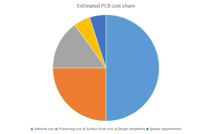
- 1) Layer Count and Copper Thickness: The more layers, the more complex the manufacturing process, requiring more lamination, drilling, and inspection steps, leading to an exponential increase in cost. Similarly, thicker copper foil (e.g., 2oz or 3oz) increases material cost and etching difficulty.
- 2) Board Size and Panelization: A larger board requires more raw materials, and fewer boards can fit on a standard production panel, which reduces panel utilization and increases the cost per board.
- 3) Trace Width/Spacing: Smaller trace widths and spacing require more precise exposure and etching equipment, and the yield is lower, so the cost is higher.
- 4) Hole Count and Diameter: Drilling is a time-consuming and labor-intensive process. The more holes, the longer the drilling time; the smaller the hole diameter, the higher the required equipment precision (e.g., laser drilling), and the higher the cost.
- 5) Microvia Layers: Microvia technology is used for high-density boards, and its manufacturing requires expensive laser drilling and repeated electroplating/lamination cycles. The more layers, the geometric increase in manufacturing difficulty and cost.
- 6) Controlled Impedance: This requires strict control of trace width, spacing to the reference layer, and dielectric constant, which increases manufacturing complexity and testing costs.
- 7) Surface Finish: Different surface finishes have different costs. For example, ENIG (Electroless Nickel Immersion Gold) is popular for its excellent solderability and flatness, but its cost is usually higher than HASL (Hot Air Solder Leveling).
- 8) Solder Mask Opening Density: The precision of solder mask openings and the minimum width of solder mask dams affect manufacturing yield and cost.
- 9) Testing Strategy: The cost of a custom test fixture (Bed-of-nails) is high, but in high-volume production, it can be amortized through extremely high efficiency. A flying probe test is more suitable for small-batch production due to its flexibility.
- 10) Data Format Maturity: Using unified formats like IPC-2581 or ODB++ can reduce data handover errors and data processing time, thereby shortening the overall lead time.
2. Practical DFx Checklist and Quoting Logic
The essence of a quote is an evaluation of the match between design complexity and the manufacturer's process capabilities. When design parameters exceed the manufacturer's standard capabilities, the yield will be significantly lower. To ensure delivery, the manufacturer will use more expensive processes or include a higher scrap cost, and these costs will ultimately be passed on to the customer.
Therefore, a practical DFx checklist can help engineers make purposeful optimizations during the design phase:
- Trace Width/Spacing: On the premise of meeting electrical performance, try to widen the traces and spacing. For example, widening from 4 mil to 5 mil can significantly improve yield and reduce costs.
- Drilling: Use standard-sized drill holes and avoid using holes that are too small or too numerous.
More PCB Manufacturing Videos at https://www.youtube.com/@Nextpcb
- Stack-up: Choose the minimum number of layers that meet the design requirements.
- Panelization: Communicate with the manufacturer to optimize the board size and shape to maximize the utilization of the production panel.
- Test Points: In the design phase, reserve sufficient test points and follow the specifications for test point size and spacing to facilitate ICT testing and reduce later debugging costs.
XI. Sustainability and Compliance Communication: ISO 14001, Environment, and Occupational Health
In an era where ESG (Environmental, Social, and Governance) is increasingly valued, sustainable development in the PCB manufacturing industry is no longer an option but a reflection of corporate responsibility and competitiveness.
1. ISO 14001 Environmental Management System (EMS)
ISO 14001 is an internationally recognized environmental management system standard that provides a framework for organizations to identify, control, and continuously improve their environmental impact. For a PCB manufacturer, implementing the ISO 14001 system not only ensures compliance with increasingly strict environmental regulations but also brings tangible benefits to the company through:
- Improved Resource Efficiency: By managing waste liquids, solvents, and energy consumption, manufacturers can identify waste points and reduce operational costs.
- Risk Mitigation: Establishing an EMS helps companies identify and assess environmental risks, thereby avoiding legal risks and reputational damage caused by environmental non-compliance.
- Market Competitiveness: More and more customers, especially large OEM manufacturers, are considering ISO 14001 certification as an important factor in their procurement decisions, which gives companies a competitive advantage.
2. Key Points of Environmental and Occupational Health
The PCB manufacturing industry has various environmental impacts, and its sustainability practices mainly focus on the following aspects:
- Waste Liquid and Solvent Management: Chemical waste liquids and cleaning solvents generated during the manufacturing process must be handled in compliance with regulations to prevent environmental pollution. This includes proper treatment of heavy metals, acids, and other harmful substances.
- Lead-Free/Halogen-Free Selection: In material selection, prioritize the use of lead-free solder and halogen-free substrates that comply with RoHS/REACH requirements to reduce the product's potential harm to the environment and human health. > Lead vs Lead-free Solder - An Ultimate Guide - NextPCB
- Energy Consumption Management: Reduce energy consumption in the production process by optimizing production equipment, improving processes, and adopting energy-saving technologies.
- Product Lifecycle: ISO 14001 emphasizes responsibility for the entire product lifecycle, which means that companies must consider the recyclability and ease of disassembly of the product in the design phase to prepare for the recycling and disposal of Waste Electrical and Electronic Equipment (WEEE).
3. ESG Communication in Customer Audits
In ESG audits conducted by customers or third parties (such as EcoVadis), manufacturers often need to prove the effectiveness of their environmental and occupational health management systems. Common audit focus points include:
- Compliance Documents: Provide legal compliance documents and records for waste liquid treatment, waste recycling, and emissions.
- Data Monitoring: Show monitoring data for energy consumption, water usage, and waste generation, as well as trends of continuous improvement.
- Employee Training: Provide records of employee occupational health and safety training to ensure that all operators understand and follow the relevant operating procedures.
XII. Glossary and Further Resources
The following glossary organizes the key industry standards cited in the report and provides brief descriptions of their purpose and authoritative sources, offering a convenient quick reference guide for readers.
|
Standard Name |
Full Name (English) |
Purpose Description |
Field of Application |
|
Acceptability of Printed Boards |
Acceptability of Printed Boards: Provides visual inspection standards with images and illustrations to judge whether bare board visual defects are acceptable |
Bare Board Manufacturing |
|
|
Qualification and Performance Specification for Rigid Printed Boards |
Rigid Printed Board Performance and Qualification: Specifies the performance requirements for bare boards in electrical, mechanical, and environmental aspects. It is a core standard for high-reliability products |
Bare Board Manufacturing |
|
|
Acceptability of Electronic Assemblies |
Electronic Assembly Acceptability: Provides visual acceptance criteria for solder joints and component placement. It is a global quality guide for the electronics assembly industry |
PCB Assembly |
|
|
Requirements for Soldered Electrical and Electronic Assemblies |
Soldering Requirements: Specifies the materials, methods, and process requirements for soldering electrical and electronic assemblies |
PCB Assembly |
|
|
Handling, Packing, Shipping and Use of Moisture, Reflow, and Process Sensitive Devices |
Moisture Sensitive Device Control: Specifies the handling requirements for moisture-sensitive components, including moisture-proof packaging, dry baking, and workshop life |
Supply Chain & Assembly |
|
|
Qualification and Performance of Electrical Insulating Compound for Printed Wiring Assemblies |
Conformal Coating Qualification: Specifies the performance and qualification requirements for conformal coating materials to ensure they effectively protect PCBAs |
PCB Assembly |
|
|
Rework, Modification and Repair of Electronic Assemblies |
Rework & Repair: Provides standardized operational guidelines for the rework, modification, and repair of electronic assemblies |
PCB Assembly |
|
|
Generic Requirements for Digital Product Model Data Exchange |
Digital Product Model Exchange: A unified data transfer format that can integrate all information for bare board manufacturing and assembly into a single file |
Design & Manufacturing |
|
|
Resistivity of Solvent Extract |
Resistivity of Solvent Extract (ROSE): A test method used for a quick assessment of the total ionic contamination on a PCBA |
Test & Inspection |


