In high-power and high-frequency electronics, effective thermal management is vital for reliability, performance and longevity. Traditional PCBs with fibreglass epoxy substrate often struggle with heat dissipation, leading to premature failure in demanding environments.
Copper core PCBs represent a specialized category within metal-core printed circuit boards (MCPCBs), distinguished by their use of a solid copper substrate rather than conventional FR4 materials. By taking advantage of copper’s exceptional thermal conductivity (approximately 400W/mK), copper PCBs offer 5 to 15 times better thermal management compared to aluminum-based PCBs.
NextPCB's manufacturing expertise in this domain encompasses sophisticated fabrication techniques, including precision z-axis milling for controlled-depth cavities and advanced pedestal techniques to maximize thermal transfer. > See capabilities directly.
What are Copper-Core PCBs?
Copper-core PCBs are metal-core PCBs (MCPCB), also known as insulated metal substrate (IMS) PCBs, that utilize copper metal for their base instead of fiberglass or aluminum.

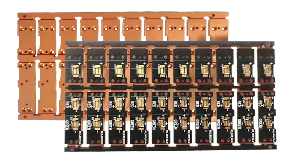
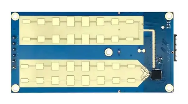
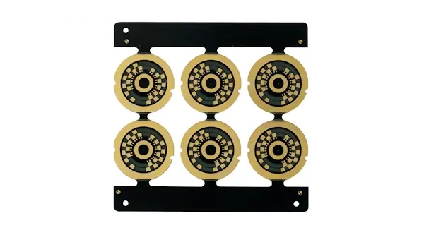
Single-layer copper core PCB panel with black solder mask and ENIG solder finish
Application - High Power LEDs
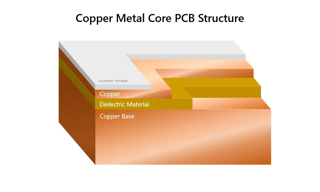
Structure of Copper-Core PCBs
Plain copper-core substrates share the same basic structure as other metal-core PCBs as shown below, where the circuitry is separated from the copper base by a thin thermally conductive prepreg layer. Although prepregs with low thermal resistance are used, the dielectric barrier has a significant impact on the overall thermal conductivity of the laminate, limiting IMS PCBs to less than 10W/mk.
Unlike aluminum PCBs, however, copper PCBs are highly compatible with pedestal technology, allowing for direct contact with the thermal pads of heat-generating components and maximum utilization of the metal’s high thermal conductivity.
Pedestal Technology
Copper pedestals can be constructed via etching or plating methods. The etching process involves selectively removing material from the metal substrate, leaving only the desired copper pedestal structures. The dielectric layer, pre-fabricated with holes aligned to the pedestal locations, is then laminated onto the copper base.
With this method, the pedestal openings in the dielectric are oversized to accommodate for registration tolerance. This creates gaps between the pedestal and dielectric, reducing reliability with repeated thermal cycling.
Plating methods remove this vulnerability by starting with the bonded substrate and removing dielectric material for the pedestal locations, then plating up copper thickness. This ensures the holes are completely filled, however, the process is slower and more expensive.
Advantages of Copper PCBs
Higher Thermal Conductivity than Aluminum
Copper metal offers superior thermal conductivity properties out of the two most common IMS metals, aluminum and copper, with a thermal conductivity 2-3 times that of aluminum. As pure substrates, thermal conductivity values are comparable and depend on other factors such as the type of dielectric material used, however, pedestal technologies allow copper core PCB’s thermal properties to elevate to much higher levels and take full advantage of copper’s high thermal conductivity.
Hardness and Durability
Copper’s inherent hardness provides exceptional structural integrity and stability through repeated thermal cycles, making it far more reliable compared to Aluminum in demanding applications. Additionally, this rigidity enables precision machining, necessary for creating copper pedestals efficiently. In contrast, aluminum's relative softness requires costly workarounds to implement pedestal technology, thereby limiting its thermal management capabilities.
EMI Shielding
With a solid copper layer extending across one side of the PCB, the substrate doubles as an EMI shield, protecting sensitive circuits from electromagnetic interference.
When to Choose Copper PCBs?
Copper core PCBs are ideal for simple designs with exceptionally high thermal requirements and few size and weight restrictions. For best effectiveness, pedestal technology should be implemented in thermal hotspots to fully utilize the metals' high thermal conductivity properties.
For higher circuit densities, such as multilayer and HDI (blind/buried vias ) designs, when heating is concentrated in specific areas, copper coin technology or copper embedding can be considered. This involves inserting pre-machined slugs of copper into standard FR4 PCBs, acting as internal heatsinks to spread heat from high-power components.
For cost-sensitive designs and designs with weight considerations, aluminum metal-core PCBs offer significant advantages over copper.
When exceptionally high thermal conductivities are required without the weight or bulkiness of metal-core PCBs, ceramic PCBs are a worthy consideration, offering a wide range of properties suitable for the most demanding environments.
>> Relevant reading: Ceramic PCB vs FR4 vs Metal-Core: Substrates for Thermal Management
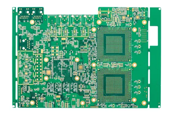
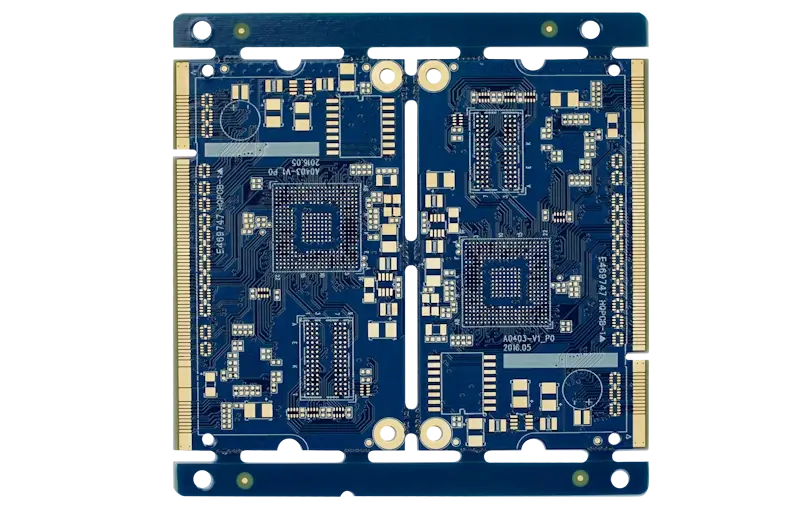
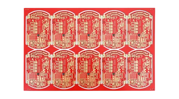
NextPCB Copper PCB Manufacturing Capabilities
| Specification |
Capability |
| Structure |
Single-sided, double-sided, multilayer base, pedestal copper core PCBs |
| Material Brands |
Shengyi, Totking and more
See below for more information |
| Thermal Conductivity |
1 to 5 W/mk |
| Max Dimensions |
1200 x 540 mm |
| Board Thickness |
0.4 to 3.0 mm |
| Copper Weight |
0.5 to 4 oz (140 μm) |
| Min. Trace Width/Spacing |
4/4 mil |
| Drill and Via Capabilities |
- Plated through holes, vias and slots (insulated)
- Blind/buried vias
- Counterbore/countersunk holes
- Z-axis milling and more
|
| Min. Hole Size |
0.3 mm |
| Surface Finish |
ENIG, OSP |
| Solder Mask |
Green, White, High Reflectivity White, Black, Matte Black |
| Extras |
Pedestal technology (etched and plating methods) |
| Industries & Applications |
- Smart Lighting: High-power LED arrays and displays
- Power Electronics: Power converters, motor drivers, SMPS
- Automotive Electronics: Headlights, BMS, ECUs
- Industrial Equipment: High-power RF amplifiers, servo drives
- Consumer Electronics: Audio amplifiers, PC cooling modules
- Aerospace: Avionics cooling systems, communication devices
|
Get an instant quote
Please inquire for advanced capabilities.
Copper-Core PCB Materials available at NextPCB
Below are some of the most common copper-core materials we support. Contact us for more information and other materials, including stainless steel and iron.
| Material Code |
Brand |
Type |
Thermal Conductivity
(W/mK) |
Tg (℃) |
Data Sheet |
| SCR20S |
Shengyi |
Copper |
2.1 |
160 |
SCR20S.pdf |
| T511 |
Totking |
Copper |
3.0 |
100 |
T511.pdf |
| T512 |
Totking |
Copper |
4.0 |
100 |
T512.pdf |
| T512C |
Totking |
Copper |
5.0 |
130 |
T512C.pdf |
Whether you're designing high-power electronics, RF/microwave systems, or high-intensity LED arrays, maximize thermal transfer in your copper-core design with NextPCB’s advanced capabilities today. Get a quote online or talk to us about your needs.

 NextPCB Capabilities
 PCB Assembly
 Layer Buildup
 SMD-Stencils
 PCB Design-Aid & Layout
 Mechanics
 Surface
 Quality
 Drills & Throughplating
 Factory & Certificate