


 NextPCB Capabilities
 PCB Assembly
 Layer Buildup
 SMD-Stencils
 PCB Design-Aid & Layout
 Mechanics
 Quality
 Drills & Throughplating
 Factory & Certificate





Introduction: Why Via Protection Matters in PCB Manufacturing
In the complex world of PCB manufacturing and PCB assembly (PCBA), vias are the vital lifelines connecting different layers of a circuit board. However, if left exposed (uncovered), these small holes can become a source of significant failure during the soldering process.
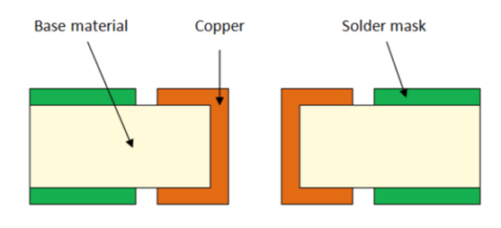
The most common issue with exposed vias is solder wicking. During reflow soldering, molten solder paste can be drawn down into the via hole through capillary action. This "theft" of solder leaves insufficient paste on the actual component pad, leading to weak solder joints, open circuits, or even tombstoning. Furthermore, exposed vias can cause accidental short circuits if they are too close to component pads.
As we move into 2026, with electronic designs becoming denser and component pitches shrinking (often below 0.5mm), choosing the right via protection method is a critical reliability decision. This guide breaks down the three primary techniques: Tenting, Plugging, and Filling (VIPPO).
Understanding IPC-4761 Standards
The industry standard IPC-4761 (Design Guide for Protection of Printed Board Via Structures) categorizes via protection into seven types. It was first released in 2006 and remains the current governing standard — there has been no newer revision. Understanding these seven types helps you specify exactly what you need in your Gerber files, avoiding delays in your turnkey PCB orders.
- Type I (Tented): Covered with mask on one side.
- Type II (Tented): Covered with mask on both sides.
- Type III (Plugged): Partially filled with non-conductive material.
- Type IV (Plugged & Covered): Plugged and covered with mask (Wet/Wet).
- Type V (Filled): Completely filled with non-conductive material.
- Type VI (Filled & Covered): Filled and covered with mask (Liquid/Dry).
- Type VII (Filled & Capped): Filled, plated over, and capped (VIPPO).
Not sure which type your current design actually uses? You can check an existing design with our HQDFM design analysis tool before deciding whether to change anything.
Method 1: Via Tenting (The Cost-Effective Standard)
Via tenting is the most basic and low-cost via protection method. It involves bridging the solder mask material (LPI — Liquid Photoimageable) over the via hole, creating a "skin" over the opening.
There are two common ways to implement via tenting:
1. Single-Sided Tenting
Vias are closed on one side and remain open on the other side of the PCB.
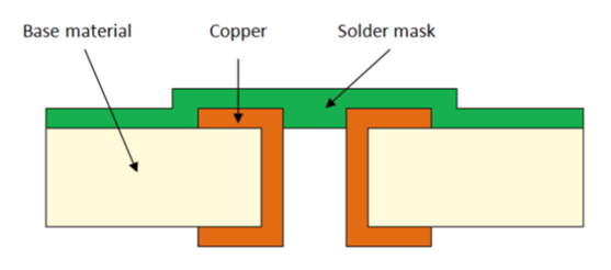
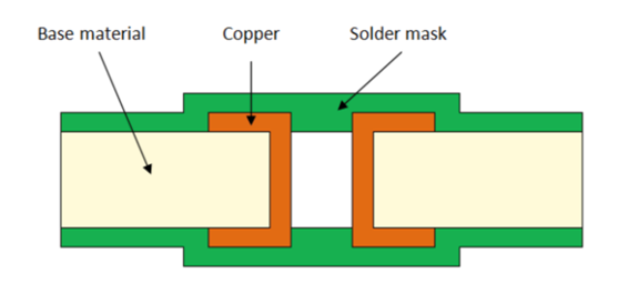
2. Double-Sided Tenting
Vias are covered with solder mask on both sides of the PCB.
For a closer look at when tenting is the right call versus when it isn't, see our via tenting design rules guide.
Method 2: Via Plugging (LPI Mask)
Via plugging means the via is partially filled with non-conductive media such as epoxy/resin or solder mask ink. This is more robust than tenting.
1. Partial Plug (One Side Open)
The via is partially filled and overprinted with conventional solder resist from one side, while the other remains open.
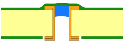
2. Full Plug (Both Sides Covered)
Filling the via with non-conductive media and overprinting it on both sides of the PCB.
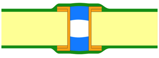
Technical note: The diameter of plugged vias should typically be smaller than 0.5mm. For multi-layer PCBs, one-sided plugging is often recommended because encapsulated gas in double-sided plugged vias can expand and cause cracks during high-temperature soldering.
Method 3: Via Filling & Capping (VIPPO)
For high-reliability designs, especially for Via-in-Pad solutions, via filling is essential. This prevents solder paste from being sucked away from the pad into the via hole.
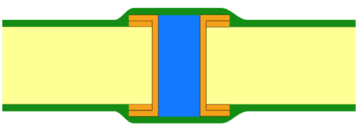
1. Complete Via Filling
The via is filled completely with non-conductive paste and overprinted with normal solder mask/paste.
2. Via Filling & Capping (VIPPO / POFV)
This is the most advanced method. First, the via is plated and cleaned, then non-conductive paste is pressed in and hardened. Finally, the ends are planarized and plated over with copper to create a flat, solderable surface.
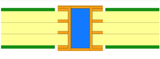
This technology facilitates additional routing traces among BGA vias and is applicable to stacked micro-vias and blind vias.
Comparison: Cost vs. Reliability vs. Application
| Feature | Via Tenting | Via Plugging (LPI) | Via Filling (Resin/VIPPO) |
|---|---|---|---|
| Relative Cost Impact | Low (Standard) | Moderate | Highest |
| Reliability | Standard | High | Ultra-High |
| Solder Wicking Risk | Moderate | Low | Zero |
| Best Application | General Consumer Electronics | ICT Test Points | HDI, BGA Designs, Aerospace |
Exact cost impact varies by via size, count, and volume, so the ranges above are directional rather than fixed quotes. For pricing specific to your board, get an instant quote with your via protection requirements noted in the fabrication notes.
DFM Guidelines: How to Design for Manufacturing
- Specify in Gerbers: Clearly indicate via protection requirements in your fabrication notes or a separate mechanical layer.
- Via size: For resin filling, keep via diameters between 0.2mm and 0.5mm for optimal results.
- BGA areas: Always consider Via-in-Pad (VIPPO) for BGA pitches under 0.65mm to save space and ensure assembly yield.
Before you submit your files, run them through our HQDFM design analysis tool or check the rendered output in our free online Gerber viewer to confirm your via protection settings match what you intended — this is the single most common source of delays we see at this stage.
Frequently Asked Questions (FAQ)
1. What is the difference between conductive and non-conductive via filling?
The primary difference lies in thermal conductivity and the Coefficient of Thermal Expansion (CTE). Non-conductive via filling uses a special epoxy resin that closely matches the CTE of the PCB laminate (FR4), reducing the risk of barrel cracks during thermal cycling. In contrast, conductive via filling uses epoxy loaded with silver or copper particles to improve thermal dissipation. Despite the name, non-conductive fill is preferred for most signal vias because the via barrel is already plated with copper for electrical conductivity, and resin provides better mechanical stability.
2. Why is Via-in-Pad Plated Over (VIPPO) necessary for HDI PCBs?
VIPPO is essential for High-Density Interconnect (HDI) boards because it allows vias to be placed directly on component pads without causing solder defects. In standard designs, a via near a pad must be connected by a short trace ("dog-bone"). With shrinking BGA pitches (0.5mm or less), there is no room for these traces. VIPPO fills the via and caps it with a flat copper surface, preventing solder from wicking down the hole and ensuring a reliable surface for SMD component mounting.
3. How does via tenting affect PCB assembly (PCBA) yield?
Via tenting can significantly impact assembly yield if the solder mask "tent" breaks or is inconsistent. If a via is improperly tented, solder paste can migrate from the SMT pad into the via during the reflow process, a phenomenon known as solder wicking. This often leads to insufficient solder or dry joints on critical components like BGAs and QFNs. For high-reliability PCBA, switching from tenting to via plugging or filling is recommended to guarantee zero solder loss.
4. Does via plugging or filling increase the cost of PCB manufacturing?
Yes. Via plugging and filling both add cost over standard tenting, since they require additional material, curing, and (for filling) planarization and plating steps. Industry data generally puts the added cost for via filling in the range of roughly 10–30% depending on via count and volume, with plugging typically landing toward the lower end of that range and full filling and capping (VIPPO) toward the higher end. Because the exact number depends heavily on your specific board, the most reliable way to know your cost impact is to request a quote with your via protection method specified.
5. Can I use via tenting for thermal vias under a heat sink pad?
No, it is generally not recommended to tent thermal vias located under a component's exposed thermal pad. Tented vias can trap air or gasses during the reflow process, leading to voiding in the thermal solder joint. Voids act as thermal insulators, significantly reducing heat dissipation efficiency. Instead, thermal vias should either be left open (if small enough) or completely filled and capped (VIPPO) to provide a smooth, continuous thermal path.
Conclusion & NextPCB Capabilities
Every via covering type has its advantages and disadvantages. At NextPCB, we support all IPC-4761 standards to ensure your PCB prototype or mass production meets the highest quality requirements.
Ready to start your next project?
Get an Instant Online Quote for PCB Fabrication & Assembly · Engineer Consultation
About the Author

Arya Li, Project Manager at NextPCB.com
With extensive experience in manufacturing and international client management, Arya has guided factory visits for over 200 overseas clients, providing bilingual (English & Chinese) presentations on production processes, quality control systems, and advanced manufacturing capabilities. Her deep understanding of both the factory side and client requirements allows her to deliver professional, reliable PCB solutions efficiently.

