NextPCB Capabilities
Printed Circuit Boards
NextPCB Capabilities
Printed Circuit Boards
 PCB Assembly
 Layer Buildup
 SMD-Stencils
 PCB Design-Aid & Layout
 Mechanics
 Quality
 Drills & Throughplating
 Factory & Certificate
 PCB Assembly Factory Show
Certificate
PCB Assembly Factory Show
Certificate
Support Team
Feedback:
support@nextpcb.com


With so many turnkey assembly providers, one would have thought the process of exporting a Bill of Materials or BOM would be relatively straightforward. Unfortunately, with KiCad, that is still not the case. The default export will likely get rejected by your supplier or require extra post-processing to make it supplier-friendly. In this article, we cover how to generate and build a complete Bill of Materials from KiCad for various PCBA services.
The best analogy for a PCB Bill of Materials (BOM) is the shopping list for the electronic components required by your electronics product. For PCB assembly (PCBA), this includes all electronics components, whether surface-mount or through-hole, and may also include fiducial marks and test pads, even though there is generally nothing to purchase for these features. This document, and versions of it, will be used throughout production by consignment and turnkey PCB assembly providers for purchasing, assembly, testing, and quality control, etc.
A BOM may also include mechanical parts such as enclosures, fasteners, screws, and packaging and printed materials for box builds.
The contents of a BOM may depend on what it is used for, e.g. a purchasing BOM, box build BOM, production BOM. Suppliers may have their own preferences on what information to include.
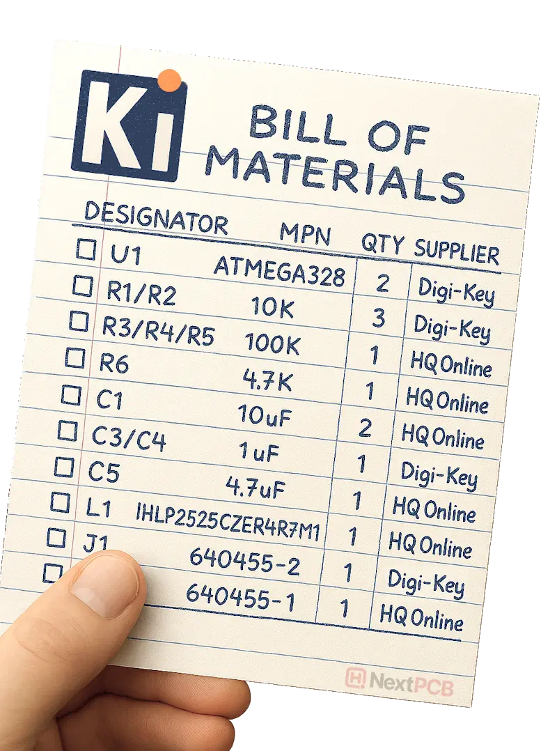
The PCB Bill of Materials (BOM), the shopping list for building electronics hardware
For consignment and turnkey services, they usually require these pieces of information at the bare minimum for each unique MPN:
Component labels assigned during schematic design for each instance of a part on the PCB design, like R1, R2 for resistors, C1, C2 for capacitors, J1, J2 for connectors. These may be the same part. Designators for the same MPN are typically grouped together in the same line in the list, often called a BOM line.
The exact component model name as given by the manufacturer. Be careful not to mix this up with the SKU (stock keeping unit) number assigned by distributors like Digikey and LCSC, as this number is only useful for that distributor.
Number of said components per board.
There are a few points to note:
Other information often included in BOMs are value, footprint, manufacturer, purchase link, supplier part number, price, alternative parts, description, etc. Additional information can be used to assist with procurement, assembly and review processes.
With the BOM, Gerber files and pick and place files, a manufacturer has all the parts of the puzzle to build the device.
Generating a working Bill of Materials ready for your supplier still feels like a bit of a workaround. Unlike Gerber files and centroid files, there is a bit of legwork required to get a usable BOM from KiCad.
The problem is that when drawing and routing your PCB, you are likely working with many generic symbols and footprints for much of your design. Many of these parts don’t have actual parts assigned to them, otherwise the library would get too big. Thus, the traditional workflow is to complete the design, then go parts shopping. Also, like other production files, data requirements differ across suppliers. Some need precise purchasing links, some need exact part numbers while others allow you to state the value for simple passive components that will use their stock. Online portals are often the most strict, requiring you to use exact headers to allow the system to recognize them.
The default KiCad BOM export supports the traditional workflow, but any change to the design is not carried over to your BOM, and you’ll have to merge the two versions each time. It is always best to have all design data centralized when possible to avoid mistakes and lost information.
Over time, KiCad has gotten smarter when it comes to BOM export, and there are various workarounds, such as scripts and plugins. KiCad’s BOM export is also highly customizable, giving various options to tailor what parts are exported and how the BOM is formatted.
Here we’ll first show you the one-size-fits-all approach to building and generating the Bill of Materials from within KiCad. This method aims to fulfill the needs of most PCB assembly houses without relying on supplier-specific plugins or tools. Then we’ll cover other strategies and compare the pros and cons of each version.
The following instructions were made in KiCad 9. Older KiCad versions and the legacy BOM format are covered where applicable.
This method works from KiCad 8 and later and requires the manual entry of the manufacturer part numbers directly into the schematic editor.
Note that both the Schematic Editor and PCB Editor have BOM export options; however, the PCB Editor export does not contain custom fields, and the export configuration cannot be edited. So it is effectively useless for procurement and production.
Before we can export the BOM, need to assign a Manufacturer Part Number (MPN) to each component symbol. This is a custom field that is not required by built-in KiCad symbols. Supplier-provided libraries may include this information for specific parts, though it is not necessary.
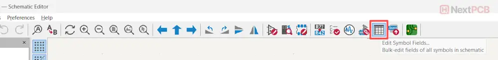
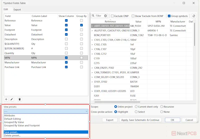
Open the Symbol Fields Table by going to Tools -> Edit symbol fields... You can also access the interface directly by clicking the shortcut button that looks like a little table on the taskbar. In the new interface, the fields table will be on the left, and a preview of your Bill of Materials will be shown on the right.
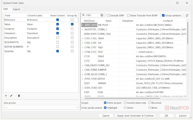
Default Symbol Fields Table interface in KiCad 9
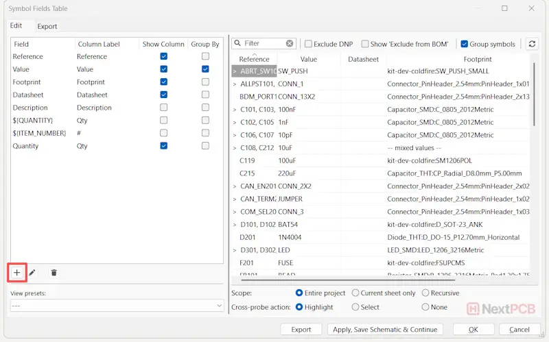
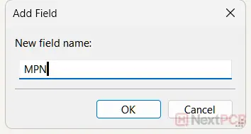
Click the plus (+) icon on the bottom left of the fields table to add a custom field. In the new window, enter MPN, Part Number, or Manufacturer Part Number, etc. These names should be recognizable by most assembly companies and automatic BOM reading systems worldwide. Then click OK. The new field will then appear in the list of fields. You can also add other fields, such as purchase link, manufacturer, or other custom fields, using the same workflow.
Check the Show Columns checkboxes for the new field to display it in the BOM preview. It will appear on the rightmost side of the table. You can move it closer to the front by dragging the header, and it is advised to do so.
Fill in the MPN values in the BOM preview table just as you would with an Excel spreadsheet.
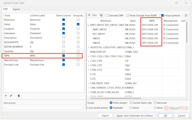
Experienced designers will know that ultimately, the BOM file should group designators by MPN. With an empty MPN column however, at this stage, grouping by MPN is not going to be useful for constructing the complete BOM. Fortunately, KiCad's Symbol Fields Table supports custom grouping by any field. This feature is invaluable in building the BOM efficiently, another advantage of filling in the BOM in KiCad rather than in spreadsheet software.
Grouping by which fields depends on at what stage of design completion you are building the BOM.
"Grouping by Value" is the default selection. All symbols must have a Value attribute which makes grouping by Value a convenient starting point. Unfortunately, this does not distinguish between capacitors of different types or package sizes for example. These can be further distinguished by adding grouping by footprint, but requires that the footprints have been selected.
After the BOM has been completed, remember to turn off grouping by Value and Footprint and turn on grouping by MPN.
Once you are ready to export the BOM and are confident the information is correct, you can prepare to export the BOM file by selecting which columns to show.
Here we list the fields typically required by manufacturers and their suggested header names for maximum success and clarity. For example, the default Reference header can be ambiguous (customer reference? Supplier reference?), so Reference Designator or just Designator is preferred. KiCad allows you to change the Column Label by clicking the text twice.
The BOM file should have at the absolute bare minimum:
|
KiCad Field |
Suggested Column Label |
|
Reference |
Designator |
|
${QUANTITY} |
Qty |
|
- none - |
MPN |
For turnkey assembly, you can also add the following to assist procurement, testing, etc. and some suppliers request it. If your service comes with DFM/DFA review, adding this information can help them quickly identify and verify the respective part. Adding all this information to your standard BOM template does not hurt, though it can clutter a BOM file.
|
KiCad Field |
Suggested Column Label |
|
- none - |
Purchase link |
|
- none - |
Manufacturer |
|
Datasheet |
Datasheet |
|
Value |
Value |
|
Description |
Description |
|
Footprint |
Footprint |
|
${DNP} |
DNP |
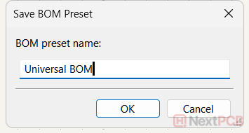
KiCad has the option to save the current settings as a preset. This allows you to create multiple templates for different purposes and manufacturer requirements, e.g. one for JLCPCB, one for NextPCB or PCBWay; for procurement, for production or testing, etc., grouped by MPN, including DNP etc. You can create a preset that assists with filling in the BOM (shows footprint, grouped by value etc.) and one for export.
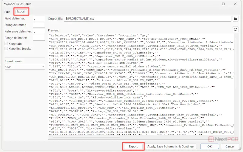
From the Symbols Fields Table Editor, you can export the BOM file by clicking the Export button at the bottom. This will save the BOM file in the directory specified above. You can also directly copy/paste the contents (excluding the headers) by selecting everything (Ctrl+A in Windows), or highlighting required sections, then right-clicking or using keyboard shortcuts.
The Symbol Fields Table interface also has an Export tab for configuring the file format and presentation of the BOM data. This includes a preview of the BOM data. This tab allows you to:
- Change the Output file directory from the default root directory
- Change the format (e.g. CSV, TSV)
- Change how fields and strings are separated (i.e. comma, tab, quotation marks)
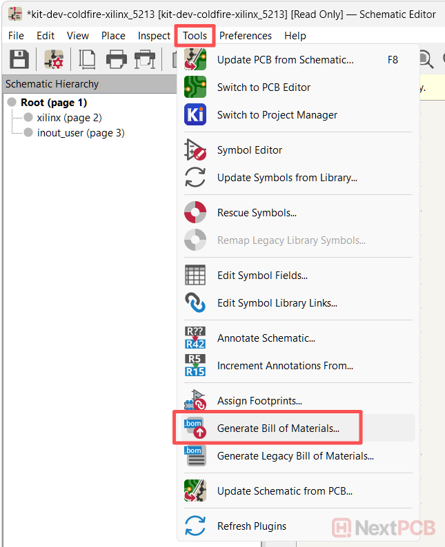
You can also go directly to the export settings from schematic view by going to Tools -> Generate Bill of Materials... There is also a shortcut button on the main menu that opens the Export tab of the Symbols Field Table interface directly.
Step 8: Perform DFA Review
Thought that was it? Now that you have the Bill of Materials it's time to verify your entire design with HQDFM!
The Bill of Materials is just a list of parts, right? So why not build it manually like the original PCB designers?
Yes, if you are handling a one-off design with just a handful of components, manual BOM creation may be quicker than setting up and maintaining everything in KiCad. However, this is where many of the BOM errors we see come in, which multiply as component numbers grow. Duplicates, the number of designators not matching the purchase quantity, missing values, etc., anything can happen with manual maintenance. EDA tools, however, rarely get the basic numbers wrong. And by exporting a complete BOM with minimal manual modifications from the EDA tool, you can maintain consistency and therefore reduce errors.
This does not eliminate the need to check your BOM before production, however, and such tools like HQDFM’s quick BOM checker can be lifesavers.
DNP (Do not populate): Parts that for this particular production run, for whatever reason, do not require installing on the boards should be marked as DNP. This may be because this particular version does not require them or that they will be populated separately. For example, if a manufacturer only supports surface mount assembly, through-hole parts should be excluded.
Exclude from BOM: These elements exist in the schematic and PCB layout but are not elements that require purchasing.
This is useful for:
- Test points
- Fiducials
- Mounting holes
- Logos/Graphics
- Net ties
- Solder bridges
Exclude from Board: the symbol is a schematic-only element. There is no PCB layout element to it. It does not appear in either the BOM or PCB layout. This would include off-board components like external modules, power sources and external modules and connectors.
Strictly speaking, DNP only tells the assembler not to install this part. It does not tell the procurement side whether it should be purchased. Each supplier has their own interpretation of what DNP means, and some automated order forms require these parts to be excluded from the BOM file altogether. To remove confusion, consider removing them from the BOM entirely.
For DNP and Exclude from BOM, KiCad has checkboxes in the export configuration that allow you to exclude them from the BOM.
JLCPCB’s PCBA service requires BOMs to have the LCSC SKU part numbers (beginning with C), not the manufacturer part numbers. You can either use their plugin or manually add a field for the LCSC Part Number. It is recommended to maintain a regular MPN column as well to maintain compatibility with other suppliers. A BOM file with only LCSC part numbers is only suitable for JLCPCB.
|
KiCad Field |
Suggested Column Label |
|
Value |
Comment |
|
Reference |
Designator |
|
Footprint |
Footprint |
|
- none - |
LCSC Part Number |
Interestingly, JLC does not require the quantity field, presumably since all the processing is done electronically and not by humans.


NextPCB provides PCB manufacturing and assembly services, focusing on reliability without breaking the bank. With 5 factories in China and over a decade of quick turnaround electronics manufacturing from prototype to mass production, NextPCB serves over 160 countries around the world, pairing dependable electronics hardware with exceptional service.
As a Platinum KiCad sponsor and long-term supporter of the KiCad open-source ecosystem, NextPCB's contribution spans developer funding, and hosting KiCon Asia — the largest KiCad‑focused event in the region. This KiCad Hub brings together all of our tutorials, tools, projects, and community contributions into one place, making it easier for designers of all levels to learn, explore, and build with KiCad.

Still, need help? Contact Us: support@nextpcb.com
Need a PCB or PCBA quote? Quote now


 Surface