

 NextPCB Capabilities
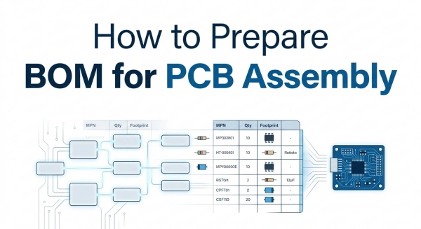
 PCB Assembly
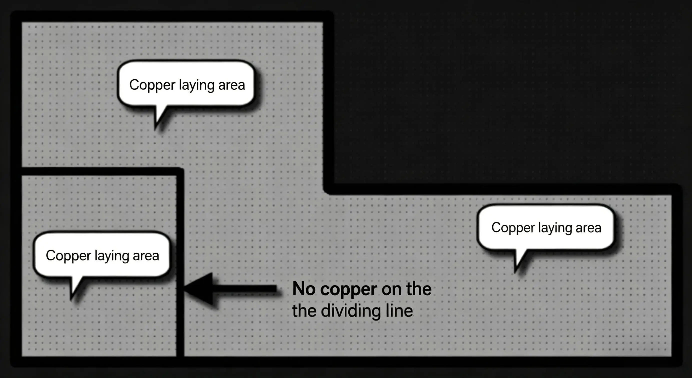
 Layer Buildup
 SMD-Stencils
 PCB Design-Aid & Layout
 Mechanics
 Surface
 Quality
 Drills & Throughplating
 Factory & Certificate


Categories
Recommended Article:
- ADAS PCB Design Guide: From Radar and Camera to Central Domain Controller Boards
- What Is Isola PCB Material? FR408HR, Astra MT77 and High-Speed Laminates Explained
- TVS Diode PCB Design: Protection Circuit Layout, Clamping Voltage and Placement Rules
- Chip Resistor Selection Guide: Tolerance, Power & PCB Footprint
- Power Inductor for AI Server PDN: Specifications and Placement Rules for Multiphase VRMs
- RF Inductor PCB Design: Q Factor, Self-Resonant Frequency and High-Frequency Layout Rules
- Ferrite Bead Impedance & Selection for High-Speed PCBs
- Inductor Saturation: What Causes It, How to Prevent It and PCB Design Rules
- Toroidal vs Drum Core vs Shielded SMD Inductor: Choosing the Right Form Factor
- Standard PCB Capabilities Compared: JLCPCB vs PCBWay vs NextPCB