
 NextPCB Capabilities
Printed Circuit Boards
NextPCB Capabilities
Printed Circuit Boards
 PCB Assembly
 Layer Buildup
 SMD-Stencils
 PCB Design-Aid & Layout
 Mechanics
 Quality
 Drills & Throughplating
 Factory & Certificate
 PCB Assembly Factory Show
Certificate
PCB Assembly Factory Show
Certificate
Support Team
Feedback:
support@nextpcb.com


The author of this article is Titov Oleg Andreevich, the owner of the Zen channel «Разумный мир». This article is the English version of «DFM, DFMA, DFA. Часть 1. Kicad и Online Gerber Viewer».
The West is very fond of various procedures and beautiful abbreviations. But in fact, these three abbreviations stand for the usual design for manufacturing and assembly capabilities:
We won't dive into the intricacies of these procedures and processes, as that would take us too far afield. Since the channel is mostly dedicated to electronics-related topics, we will only cover the design and fabrication of electronic devices. And for the most part not in the abstract, but in the example of a power module of electronic load, a link to the scheme of which I gave at the end of the article «Немного об электронных нагрузках и их особенностях».
Moreover, we will limit ourselves only to some issues related to the printed circuit board.
Why KiCad and NextPCB It's very simple, there are no secrets here:
«Design» is «Constructing» or «Designing». This can be considered partially overlapping with the term "Development", which we will use today.
«Manufacturing» is «Production». But today we will consider manufacturing to be only the process of making a printed circuit board, without installing components on it.
«Assembly» is «Assembly». We will understand assembly as the installation of components on a finished printed circuit board.
On the one hand, the device to be developed must fulfill the specified functional requirements and meet the specified parameters. On the other hand, there are always constraints in the form of the availability of various components and materials, as well as the technological possibilities of production. We have to take all this into account if we really want to get a finished electronic device, even in a single copy. Money issues and development and production times cannot be ignored either.
Let's leave the functional requirements aside for now. The remaining constraints are directly related to manufacturing issues.
There is no point in using electronic components that cannot be purchased in sufficient quantities. Less obviously, there may be additional constraints. For example, you may be required to use very specific components that are already used in other devices and are purchased in large quantities. Even if their parameters are clearly unnecessary for your device.
Reliability requirements and delivery times may also influence the choice. It is often necessary to take into account the operating conditions of the device. For example, to work under vibration conditions the components used should provide for the possibility of additional mechanical fastening.
SMD components allow to reduce the size of the printed circuit board and the whole device, but they are more difficult to install, which requires higher qualifications of installers. The chosen variant of the component housing may turn out to be inconvenient during assembly. And these are already production factors. That is, the circuit designer must choose the components used not only on the basis of design parameters but also taking into account many additional factors.
The materials used can also affect the work of the circuit designer. So the material of the printed circuit board affects the parameters of RF and microwave devices. For heat dissipation in hermetically sealed enclosures, it may be necessary to use printed circuit boards with a metal base. This affects the calculation of thermal behavior and the choice of electronic components.
But we will consider the circuit design phase complete today.
After completing the development of the circuit diagram of the device, but more often in parallel, the development of the printed circuit board begins. In this case, first of all, a lot of rules and requirements are taken into account, which are not directly related to production. These are the rules of mutual placement of components, ensuring electromagnetic magnetic compatibility, selection of copper thickness and track width depending on the current flow, mutual location and length of tracks, and much more.
But you also have to take into account the technological limitations of production. And not only for the PCB but also for the entire device. For example, there are restrictions on the minimum width of PCB tracks and the distance between them. The dimensions of the contact pads must be selected with regard to the type of mounting and soldering. For manual soldering, you need larger dimensions, and for automatic installation of SMD components and reflow soldering smaller.
The working conditions of the device are also taken into account, which may require additional mechanical fastenings of components or filling the assembled board with compound. And dimensions of the printed circuit board and the location of fixing holes, location of indication, and adjustment elements are determined by the device case.
In general, printed circuit boards are divided into several complexity classes. In KiCad you can find such a table.
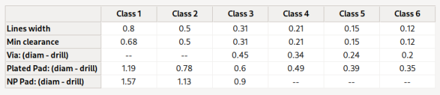
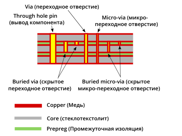
The higher the complexity class, the higher the demands placed on the accuracy of its manufacture, which affects both the cost and the manufacturing capability itself. Complex PCBs are often multilayer, which can cause additional constraints on the part of the manufacturer. For example, micro-vias holes or buried-via may not be supported. I'll repeat the illustration from my article «KiCad для начинающих §9. Начинаем знакомство с редактором печатных плат»
If you make your own PCBs, then of course you know your technological capabilities. If the PCBs are ordered somewhere, you should always know the capabilities of the chosen manufacturer. For example, for NextPCB they would be «PCB Capabilities». That's what we'll need today.
It is important to realize that technological capabilities are only a limit, not an action guide.
We will assume today that the PCB topology has already been designed. The PCB is double-sided.
KiCad PCB Editor supports «Design Rules». In general, you can simplistically think of design rules as a way to set a limit on the technological possibilities for a particular PCB, although this is not entirely true. But even if you simply compare KiCad's list of design rules with the limits specified on the NextPCB website, you'll see that not everything can be specified and checked at the KiCad level. We'll come back to this shortly.
The adherence to design rules in PCB design is partly automatic. But we can always change the rules in the process of work. In this case, the already finished part of the board will not be automatically rebuilt. This is why there is a separate «Design Rules Check» (DRC), which is usually performed after the design is completed.
It is important to realize that the design rules check only applies to the PCB in KiCad's internal format. This check has no bearing on the creation of the PCB production files. If the files for production are generated in error, or their producer is interpreted in error, the PCB will be defective. I wrote about one such case in the article «Вниманию пользователей KiCad и JLCPCB! И не только!».
Thus, doing DRC cannot fully guarantee that your PCB will not cause problems in production. Furthermore, the manufacturer cannot look into the developers' heads and find out at least the purpose of the PCB. He only has the files we provide. And there is not, and cannot be, a schematic of our device.
That is why the manufacturer always performs a check of the files provided by us. And it is no longer a check of design rules, but a check of compliance with technological capabilities. At least. Checking the same DFM. If errors are found, either you, as a customer, will be informed about them to correct the errors or the errors will be corrected by the manufacturer, which may affect the price, or the board will be made "as is" if you refused to correct the errors.
In addition, the manufacturer may not just check that your board meets their technological capabilities, but may also factor the complexity of the board into the cost of fulfilling the order.
Therefore, it is always interesting and useful to know how our board is seen by the manufacturer. This will allow you to detect and correct errors in advance, even if you do not consider them as such. And it will reduce the time of order fulfillment because there will be no unnecessary correspondence. But it can also save you money.
And this brings us directly to the topic of the article and the tools that NextPCB offers. And it offers them explicitly, literally insists on it, and for free. We will now see how these tools work and how useful they can be.
Once again, I should note that we are only interested today in tools that we, as the customer, can use to verify a PCB before placing an order. Not surprisingly, all manufacturers that provide such tools have them geared towards their capabilities. Moreover, it is usually assumed that once verified, they are the ones you will place your order with. We'll just keep that in mind.
NextPCB offers two tools that have different capabilities. Both tools can be found on the «HQDFM Free Online Gerber Viewer and DFM Analysis Tool» page.
To see the difference from the usual PCB ordering interface, we will briefly (very briefly) take a look at it. For comparison. But first, let's look at our board through KiCad's eyes.
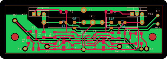
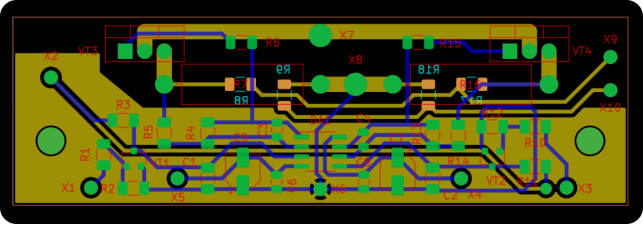
I already gave a link to the article with the schematic of the power module of the electronic load at the beginning of the article. Let's see what the PCB for this module looks like in KiCad PCB editor version 7.0.10
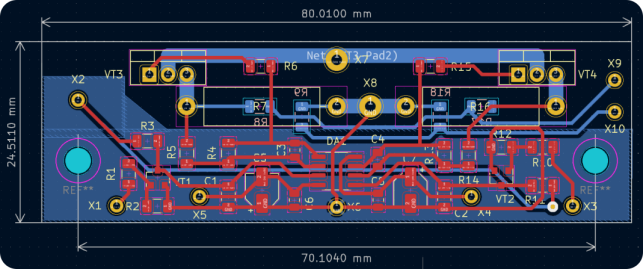
This board was designed for self-build and hand soldering but was later ordered from JLCPCB as well, and no problems were found with it. It should be noted that the origin point for the board is set to the upper left corner of the board. The coordinate origin for component placement and drilling is also located there.
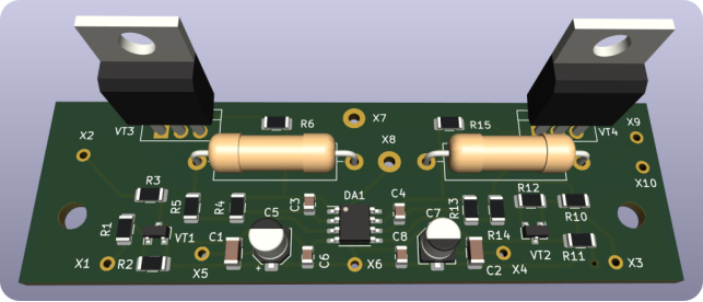
In 3D form, the board looks like this:
This will be our starting point. For the board, we have generated Gerber files with layers F.Cu, B.Cu, F.Mask, B.Mask, F.Silkscreen, and B.Silkscreen. Edge.Cuts. Drilling files NPTH.drl and PTH.drl were also generated. Let's load these files into KiCad Gerber Viewer. Our set of files will look like this
This is how our board should be seen by the manufacturer. And what we will get, we will see now.
To see how the DFM NextPCB inspection tools differ from the typical PCB ordering interface and to evaluate the feasibility of using them, let's start with the simplest one, which is the one most often used by the average customer, much less an amateur. But since I mentioned that the board was ordered (without error) on JLCPCB, let's first see how this manufacturer saw it. Let's upload our files (as a ZIP archive) in the JLCPCB order window
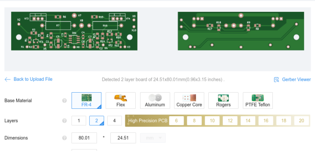
We can clearly see that there are no problems detected (although the manufacturer will perform an additional check later), the appearance is correct, and the dimensions are correct. So there really is nothing wrong with the board. Now let's download the same files on NextPCB's «Get Online PCB Quote» page. But we get a little unexpected result
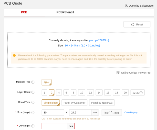
For a moment images of two sides of our board appear, which show that the manufacturer has seen everything correctly, but then these images disappear and instead of them there is a notification asking to check the board parameters automatically obtained from Gerber files. At the same time, everything is defined correctly, there are no errors, you can simply select the number of boards and the order will be formed. To make it clearer, I have recorded a small video.
At the same time, just below the window where the PCB image should be, there is a link to "Online Gerber Viewer Pro". This hints quite transparently that we are strongly encouraged to use one of NextPCB's DFM verification tools. Or we can just place an order if we have had time to look at the board and are sure there are no errors. True, the Pro supplement appeared here, but it is exactly the same tool.
We can simply click on the link, and we will see the Online Gerber Viewer window with the files we have already downloaded, or go to the «HQDFM Free Online Gerber Viewer and DFM Analysis Tool» page through the site menu and download our archive with the files. The result will be absolutely identical. This is what it looks like in the browser
In the middle of the screen, we see our board, although it doesn't look exactly like in KiCad. On the left is the layer selection window, but some of the layers are switched off. The behavior of the layer selection window is not quite familiar. We can only switch a layer off or on, it is done by a single click. A double click switches off all layers and switches on the specified one. Let's switch on all layers by clicking the «Open All» button above the layer list. Now our board looks almost similar to KiCad Gerber Viewer
But the pin holes are not visible. Let's fix this by clicking twice, with a small pause between clicks, so that it is not perceived as a double click, on the Drl layer. Now it's quite similar

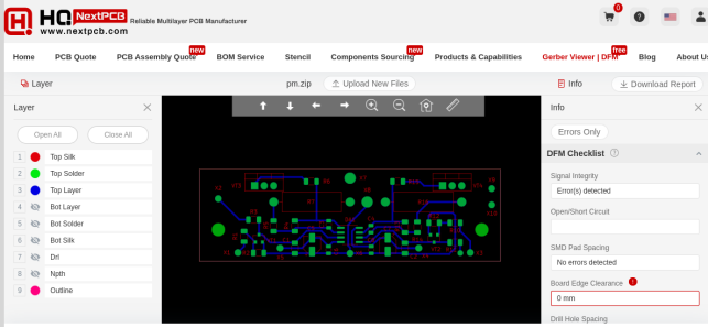
But did the manufacturer really not find any errors? Alas, they did. To the right of the window with the board image, there is a window with various information, including detected errors. Here it is, the found error
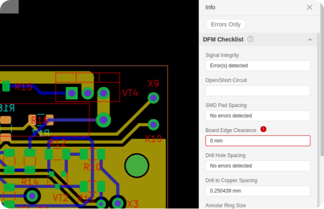
It is marked with an exclamation mark in a red circle and «Board Edge Clearance» is highlighted with a red frame. That is, the copper (polygon, track, contact pad) is too close to the edge of the board. Alas, there are no additional hints and there is no possibility to find the problem spot. But if you hover your mouse over the exclamation mark, you will see a small window with a hint - «download the DFM test report file». Above the window with information there is a button «Download Report», by clicking on it we will download a file with the name «report.pdf» (the name does not change). After opening it we will finally see not only information about our board but also its image.
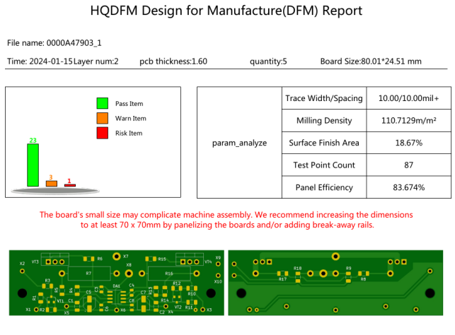
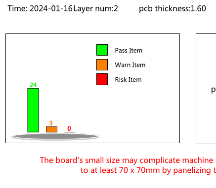
The same one that appeared briefly in the board ordering interface. You can see that the board looks correct, but the manufacturer found 1 error (Risk Item) and 3 locations that may cause problems but are not errors (Warn Item). It's already getting more interesting. Let's see what the error is, to do this, let's scroll through the file further. And we will see this interesting information in the table (here is a small fragment)
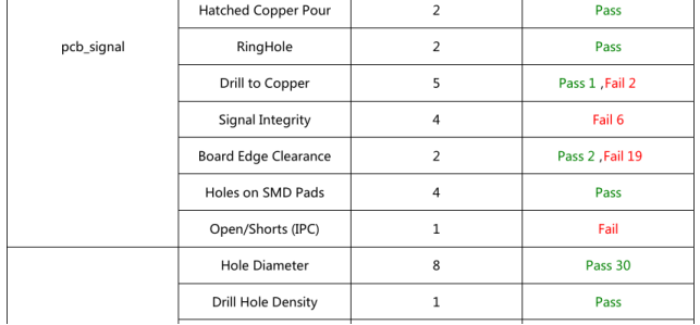
Let's take the line with the «Board Edge Clearance» check because this is the error that was detected. We can see that as many as 19 items caused problems. And this is strange at least. After all, there is only one error, but there are 3 more warnings. It is even more interesting that there are 5 rows with errors in this table, not 4. But let's find the error detected by NextPCB Online Gerber Viewer and scroll through the report file further. And we will see what we are looking for
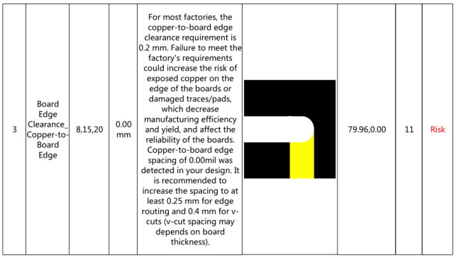
The last column unambiguously indicates that this is an error (risk). The third column (8, 15, 20) contains a list of violated rules, which does not help us in any way, as we could not find these rules (and numbered). There is also a column explaining why this is considered an error and how it can be corrected. There are also coordinates of the problematic place (79.96,0.00), but we cannot use them, because NextPCB Online Gerber Viewer does not show the cursor coordinates.
But the most interesting thing is not that, it says here that there are 11 such problem places, not 19, as we saw in the previous table. At the same time, the coordinates are given only for one point, not 11. It is a mystery... And it is not clear how to search for the other points. But we'll try anyway.
Let's return to KiCad Gerber Viewer. We have set the origin of coordinates for the board in the upper left corner. It is logical to assume that in the table in the report file, the coordinates are counted from this point. Let's choose a small enough grid, for example, 0.1 mm, and look for the point with coordinates (79.96,0.00). In this case, it is quite simple, it is the upper right corner of the board, but in general, the position of the problem point will not be so obvious. But there is no copper at this point, so what's the catch? Have the Gerber files been generated incorrectly?
No, everything is formed correctly, it is our error, the notorious "human factor". That's where it's hiding
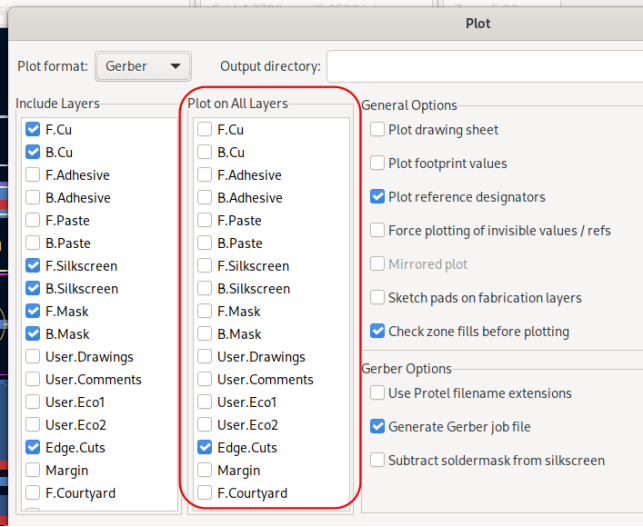
I have circled the cause of the error with a red frame. When forming Gerber files, drawing of Edge. Cuts layer on all layers was enabled. I used old Gerber files, which were formed for self-made boards so that the edges of the board were highlighted as a copper track. This is the track that NextPCB saw as an error. Let's fix the error and check it again
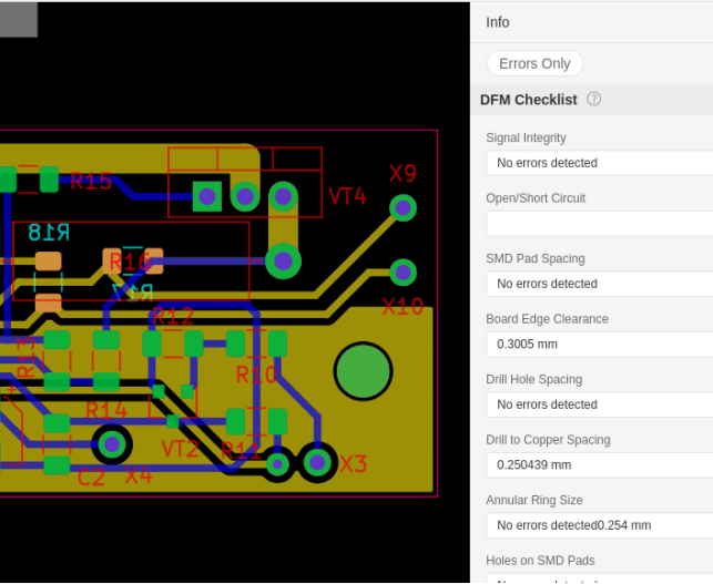
The error is gone. The 0.3 mm distance from the copper to the edge of the board is now correct. But let's check the report file, is everything OK there?
Yes, the error is gone. But the warnings are still there. And there are also 3 problematic places with Board Edge Clearance, only now in the form of warnings. But the coordinates are again specified only for one point
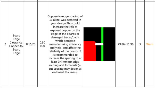
Warnings can be ignored, but let's try to understand. In the description of the problem and how to fix it it is stated that it is recommended to increase the gap between the copper and the edge of the board up to 0.4 mm. We have only 0.3, which is set through Kicad design rules. And DRC did not detect this problem, which is quite natural. In fact, the 0.4 mm is clearly a result of NextPCB's technological capabilities (PCB Capabilities). I warned you that we would still need them today, didn't I? This is described in two paragraphs:
But the coordinates of the problem point look strange, where did the minus come from? In KiCad Gerver Viewer all coordinates for our board are positive. The reason is quite simple, the directions of coordinate axes in KiCad and NextPCB are not exactly the same. The X-axis in both cases is directed from left to right, but the Y-axis in KiCad is directed from top to bottom, and in NextPCB from bottom to top, as in the Cartesian coordinate system at school. That's why the Y coordinate signs are different.
Now in KiCad Gerver Viewer, it is easy to find the problem point, but I think you have already guessed that it is a polygon (Gnd) on the B.Cu layer. If we increase the gap between the copper and the board edge in KiCad design rules to 0.4 mm and re-fill the polygons, the warning disappears. Anyway, this is a warning.
Let's consider the next warning very briefly. It concerns fixing holes, where the distance from the edge of the hole to the same polygon turned out to be 0.25 mm
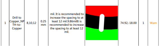
It's just that circles in KiCad are approximated by line segments (you can see it at high magnification), that's why the distance was only 0.25 mm, not 0.3 mm (which was not detected by DRC, of course). Design rules will not help here, we have to use keep-out zones.
Let's postpone the analysis of the remaining two lines with Fail results (Open/Shorts (IPC) and Fiducials) for now. Firstly, there is no additional information on them, not even coordinates. Secondly, the article is already too large. Therefore, we will deal with them already in the PC program, which is more functional, though not without disadvantages.
That's enough for today! We will consider the «NextPCB DFM Analysis Tool» program, which is more interesting and functional, in the next article.
So, we managed to find and fix the error and problem places, albeit not without difficulty. And we did it on our own, without correspondence with the manufacturer, which saves time (and sometimes money). However, I had to use not only NextPCB Online Gerber Viewer but also KiCad Gerber Viewer.
So we can admit that the Online Gerber Viewer tool offered by NextPCB is useful, but far from being the most convenient. It allows you not only to see how the PCB looks from the manufacturer's point of view but can help you to find errors. It would be much more convenient if the problem places were somehow marked directly in the PCB viewer window. Even if the detailed explanation will be in the report file. And the report file itself not only contains contradictory information but also useful information that is far from complete. Coordinates of problem points, at least.
Will these flaws and errors be corrected? Time will show. I don't consider the lack of Russian language to be a problem, but I know that it is a problem for many people. What is really missing is a list of rules referenced in the report and a user manual. A professional will certainly understand but will use the program rather than the online tool. But for a novice or amateur, it can easily become an insurmountable obstacle.
Online Gerber Viewer is useful, but very controversial. At the same time, we are literally pushed to use it if we order PCB manufacturing from NextPCB. But still, it is not necessary to use it. However, everyone decides for himself. I just showed you what it is. And the programme... That is already in the next article.
you may also be interested in....
Still, need help? Contact Us: support@nextpcb.com
Need a PCB or PCBA quote? Quote now


 Surface

