What are High-Frequency PCBs?
High-frequency PCBs are specialized printed circuit boards designed to carry high-frequency RF, microwave, and millimeter-wave electromagnetic signals, typically ranging from 300 MHz to 110 GHz. While standard PCBs are often optimized for cost and structural integrity, high-frequency boards are engineered specifically for signal integrity and minimal interference. As data transmission speeds increase, the physical properties of the board material—such as the substrate and copper foil—become a critical, active part of the electrical circuit itself.
To maintain performance across such a vast spectrum, these boards require strict circuit layout discipline and specialist materials that address three main technical pillars:
- Low Dissipation Factor (Df): This minimizes signal power loss as heat within the board material, ensuring the signal reaches its destination with maximum strength.
- Stable Dielectric Constant (Dk): The speed of a signal depends on the Dk of the material; high-frequency boards require this value to remain consistent across different temperatures and frequencies to prevent timing errors and phase shifts.
- Low Moisture Absorption: Because even trace amounts of humidity can alter electrical properties, high-frequency materials are designed to be highly resistant to moisture to maintain reliability in various environments.

Frequency Spectrum and Applications
High-frequency applications generally fall into the microwave and millimeter-wave subsets, covering the following critical ranges:
- Ultra High-Frequency (UHF: 300 MHz to 3 GHz): This range includes most consumer electronics, GPS, Wi-Fi, and 4G LTE networks.
- Super High-Frequency (SHF: 3 GHz to 30 GHz): This encompasses high-speed technologies like Wi-Fi 6, 5G mmWave, and advanced radar systems.
- Extremely High Frequency (EHF: 30 GHz to 110 GHz+): This spectrum supports cutting-edge applications including 6G R&D, military-grade satellite communications, and high-resolution automotive radar.
By utilizing specialized substrates from manufacturers like Rogers, Isola, or Taconic, high-frequency PCBs provide the thermal management and electrical precision necessary for modern telecommunications, aerospace, and medical imaging industries.
High-Frequency Applications and their Frequency Bands and Example Materials
| Application |
Frequency Range |
Band |
Example Materials |
| Wi-Fi 6/6E |
2.4 GHz, 5 GHz, 6 GHz |
SHF |
Rogers RO4835™, Isola FR408HR |
| 5G Sub-6 GHz |
600 MHz – 6 GHz |
UHF/SHF |
Megtron 6, Nelco N4000-13EP |
| 5G mmWave |
24 GHz – 100 GHz |
EHF |
Rogers RT/duroid 5880™, Taconic TLY™ |
| Automotive Radar |
24 GHz, 77 GHz, 79 GHz |
EHF |
Rogers RO3003™, Arlon AD350™ |
| Satellite Comms (L/S-band) |
1–4 GHz |
UHF/SHF |
Taconic RF-35™, Rogers RO4003C™ |
| Satellite Comms (Ka/Q-band) |
26–40 GHz |
SHF/EHF |
Rogers RT/duroid 6002™, PTFE-based |
| RFID/NFC |
125 kHz – 5.8 GHz |
LF/HF/UHF |
Standard FR4, Polyimide flex |
| Phased-Array Antennas |
6–100 GHz |
SHF/EHF |
Rogers RO4730G3™, CuFlon® |
| Military Radar |
1–18 GHz (X/Ku-band) |
SHF |
Rogers RO4830™, Arlon 25N™ |
NextPCB offers PCB manufacturing using ultra-low-loss high-frequency materials from leading laminate manufacturers and experience with hybrid stack-ups, impedance control, via backdrilling, to give you the tools to tackle signal distortions effectively. Check out our high-frequency PCB capabilities or get an instant quote.
Challenges of High-Frequency PCB Design
Designing printed circuit boards (PCBs) for high-frequency applications introduces unique challenges that do not exist in conventional digital or low-frequency analog circuits.
In addition to reflections (from impedance mismatches) and crosstalk (parasitic coupling), high-frequency signals are susceptible to dielectric losses, conductor losses (skin effect), and variable dielectric constants (dispersion).
Above speeds of 1 GHz, high-frequency effects become noticeable. By 6 GHz, high-frequency design principles and standard FR4 laminates become increasingly insufficient to meet signal integrity requirements, necessitating the use of specialized high-frequency PCB materials for controlled impedance and low loss.
As digital data-rates increase beyond 1-6 Gbps, high-frequency distortion phenomena begin to surface and become problematic in high-speed digital circuits as well. In such cases, low-Df, controlled-Dk high-frequency substrates can also be deployed to preserve signal integrity, particularly in multi-gigabit applications (PCIe, Gen4/5, DDR5, 112G SerDes).
High-Frequency PCB Routing Principles
In high-frequency environments, every trace, via, and corner behaves as a distributed circuit with specific resistance, capacitance, and inductance. Minor routing errors can lead to signal degradation, Electromagnetic Interference (EMI), or system failure. To ensure signal integrity, NextPCB follows these eight core routing principles centered on minimizing loss, suppressing radiation, matching impedance, and eliminating loops.
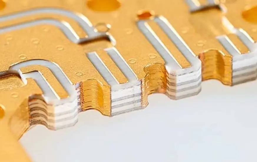
- 1) Utilize Multilayer Boards: High-frequency designs require multilayer stacks. Using internal power and ground planes provides essential shielding, lowers parasitic inductance, and significantly reduces cross-talk between signal layers.
- 2) Minimize Trace Bends: Use 45° angles or circular arcs instead of 90° corners. Sharp bends create impedance discontinuities, which lead to signal reflections and increased radiation.
- 3) Keep Traces Short: Signal radiation intensity is proportional to trace length. Critical lines, such as clock signals and DDR routing, must be kept as short as possible to prevent coupling with neighboring components.
- 4) Reduce Via Count: Every layer transition (via) introduces approximately 0.5pF of parasitic capacitance. Minimizing the number of vias maintains signal speed and reduces the risk of data bit errors.
- 5) Manage Parallel Crosstalk: Avoid long parallel runs between traces. If parallel routing is unavoidable, increase the spacing, use orthogonal routing on adjacent layers, or place a ground plane on the opposite side to isolate interference.
- 6) Strategic Decoupling: Place high-frequency decoupling capacitors as close as possible to IC power pins. This stabilizes the power supply and suppresses high-frequency harmonics.
- 7) Ground Isolation: Separate digital and analog grounds to prevent noise contamination. Connect them at a single point or through high-frequency ferrite beads to maintain a consistent ground potential.
- 8) Avoid Signal Loops: Signal traces must never form a closed loop, as these act as antennas for electromagnetic induction. If a loop is necessary, its area must be kept to an absolute minimum to reduce EMI emissions.
Material Selection for High-Frequency PCBs
In the realm of high-frequency circuitry, the requirements for signal transmission quality and speed are exceptionally stringent. Designing these PCBs goes far beyond simple physical connectivity; it necessitates a deep dive into core challenges such as signal integrity, electromagnetic crosstalk, transmission delays, and the skin effect. This process is a multidisciplinary endeavor, seamlessly integrating material science, advanced manufacturing processes, and precision testing technologies.
High-performance laminates serve as the bedrock for overcoming these technical hurdles. These materials are specifically engineered to minimize signal loss and reduce distortion at microwave frequencies, primarily through optimized dielectric constants (Dk) and extremely low dissipation factors (Df). From a material composition perspective, these high-frequency substrates are broadly categorized into PTFE-based and non-PTFE-based laminates. While PTFE is renowned for its superior electrical properties, it presents unique manufacturing challenges. Conversely, non-PTFE materials—such as Polyphenylene Oxide (PPO/PPE) and Liquid Crystal Polymer (LCP)—offer a more balanced trade-off between mechanical processability and electrical performance.
When selecting a substrate, engineers must look beyond Dk and Df to evaluate critical factors like temperature coefficients and dimensional stability, ensuring consistent performance across varying environments. Furthermore, the role of copper foil as the direct medium for signal transmission is paramount. Ideally, copper foil should offer high surface smoothness to mitigate losses caused by the skin effect, while maintaining sufficient peel strength. Coupled with high-precision etching to ensure trace width consistency, these factors work together to lock in the characteristic impedance and achieve the intended high-frequency design goals.
PTFE-based
Also known by the brand name Teflon, PTFE PCBs or Teflon PCBs are made from the polymer Polytetrafluoroethylene (PTFE) and can be reinforced with microfibers or filled with ceramic particles. The prime advantage of PTFE materials are their exceptionally low losses, stable and low dielectric constants. And are often considered the gold-standard for microwave and millimeter-wave PCBs.
Examples of PTFE-based High-Frequency PCB Materials
| Material |
Brand |
Type |
Dissipation Factor (Df) |
| RT/duroid 5880 |
Rogers |
PTFE + Glass |
0.0009 |
| RO3003™ |
Rogers |
PTFE + Ceramic |
0.0013 |
| mmWave77 |
Shengyi |
PTFE + Ceramic |
0.0010 |
Pure-PTFE laminates offer the lowest dielectric loss but are mechanically weak. Ceramic filling or fiberglass reinforcement improves mechanical and thermal stability, but at the expense of low Df.
Non-PTFE based
This includes Rogers RO4003C and RO4530B which are often mistakenly referred to as PTFE laminates. Non-PTFE options include hydrocarbon ceramics, modified epoxies and polyimides. In hydrocarbon ceramics, the ceramic particles give the material exceptional thermal conductivity, high-temperature stability and rigidity. The optimal mechanical properties make them compatible with standard FR4 PCB fabrication methods, thereby simplifying PCB fabrication significantly. Non-PTFE laminates provide cost-effective alternatives to PTFE materials and are highly suited for volume production, but can still be several magnitudes more expensive than FR4.
Examples of Non-PTFE-based High-Frequency PCB Materials
| Material |
Brand |
Type |
Dissipation Factor (Df) |
| RO4003C™ |
Rogers Corp |
Hydrocarbon ceramic |
0.0027 |
| RO4830B™ |
Rogers Corp |
Hydrocarbon ceramic |
0.0037 |
| I-Tera® MT40 |
Isola |
Hydrocarbon ceramic |
0.0031 |
| FR408HR |
Isola |
Modified FR4 |
0.0092 |
For flex and rigid-flex constructions, flexible high-frequency materials such as Pyralux TA (modified polyimide) and LCP (liquid crystal polymers) offer excellent low-loss performance while maintaining flexibility.
The main selling points of high-frequency materials are ultra-low dielectric loss and a stable dielectric constant over a range of frequencies. Ultimately, the decision of which material to use will be determined by the high-frequency performance requirements of the system while also taking into consideration factors such as Dk consistency vs temperature, CTE, temperature and moisture resistance, durability and mechanical properties, ease of manufacture, cost, etc.
NextPCB High-Frequency PCB Materials
NextPCB’s PCB manufacturing capabilities cover both PTFE and non-PTFE Rogers laminates for consumer to extremely high-frequency applications. See the table below for some of the Rogers materials we support, or see our high-speed materials for other low-loss options. Some materials are considered more popular in high-speed applications; however can also cater to high-frequency needs.
| Material Code |
Brand |
Max
Frequency |
Dissipation Factor
Df (@10GHz) |
Dielectric Constant
Dk (@10GHz) |
Tg/°C (non-PTFE)
Td/°C (PTFE) |
CTE (ppm/°C) |
Type |
Copper
Cladding |
Datasheet |
| X |
Y |
Z |
| RO4003C |
ROGERS |
30 GHz |
0.0027 |
3.38 |
280 (TMA) |
11 |
14 |
46 |
Hydrocarbon / Ceramic / Woven Glass |
ED |
RO4003C.pdf |
| RO4350B |
ROGERS |
30 GHz |
0.0037 |
3.48 |
280 (TMA) |
14 |
16 |
50 |
Hydrocarbon / Ceramic / Woven Glass |
ED |
RO4350B.pdf |
| RO3003 |
ROGERS |
77 GHz |
0.0013 |
3 |
500 (TGA) |
17 |
16 |
25 |
PTFE + Ceramic Filling |
ED + RA |
RO3003.pdf |
| RO5880 |
ROGERS |
110 GHz |
0.0009 |
2.2 |
500 (TGA) |
22 |
28 |
173 |
Reinforced PTFE |
ED + RA |
RO5880.pdf |
| RO5870 |
ROGERS |
110 GHz |
0.0012 |
2.33 |
500 (TGA) |
31 |
48 |
237 |
Reinforced PTFE |
ED + RA |
RO5870.pdf |
Get an instant quote
Or inquire for more materials
NextPCB Fabrication Services for High-Frequency PCBs
In addition to sourcing and processing high-frequency laminates, fabricators can offer many other services to optimize the performance of high-speed and high-frequency PCBs. When choosing a high-frequency PCB manufacturer, be sure to evaluate all their capabilities and experience with high-frequency PCB stack-ups, materials and supporting services.
Impedance Control
For high-frequency and ultra-high-speed digital designs, where tolerance requirements of ±5% are common, standard impedance control practices are inadequate. Test coupon validation does not take into account via stubs, plane cuts or cross-talk in real traces and TDR instruments measure impedance, not signal integrity or power integrity. For RF circuits, S-parameters and phase stability are just as important and a strategy combining simulation and on-board probing, in addition to specialist materials, are essential for optimal signal integrity.
Hybrid Stackups
The greatest downside to specialist high-frequency laminates is the cost. One way of reducing material fees is to design a hybrid stack-up that combines high-frequency laminates with standard FR4 materials. By consolidating all RF signals into a few signal layers, designers can make substantial savings compared to a full high-frequency PCB stack-up. FR4 layers can also impart favorable mechanical properties to the hybrid PCB, such as better rigidity.
For hybrid stack-ups, designers should select materials with similar CTEs and work with fabricators with experience building hybrid stack-ups to reduce the risk of delamination.
Designers choosing a hybrid stack-up should pay special attention to impedance shifts at mixed-material transitions and utilize via stitching appropriately.
Backdrilled Vias/Filled Vias
PCB backdrilling utilizes controlled-depth drilling to remove via stubs, which can be significant sources of signal reflections and losses in high-speed and high-frequency PCB designs. Via backdrilling physically removes the unwanted via excess by mechanically drilling it away from the other side of the PCB, essentially making a blind via structure. High-precision z-axis drilling techniques are required to remove enough material without damaging the functional part of the via.
Likewise, via filling with either conductive or non-conductive epoxy removes the air gap in via barrels, thereby reducing the impedance mismatch. This is advantageous in compact layouts such as dense BGA fanouts, where backdrilling is impractical.
Fine Trace Width Capabilities
For higher impedance targets, finer traces may be required to achieve the required impedance value. Finer trace width capabilities allow for optimal impedance matching without compromising for production limitations. Finer traces also allow for minimal dispersion, which becomes essential in mmWave frequencies (>30 GHz).
NextPCB High-Frequency and High-Speed PCB Manufacturing Capabilities
| Capability |
Details |
| Stack-ups |
Custom hybrid multilayer PCB stack-ups |
| Materials |
High-Speed PCB materials
Low-Dk and Low-Df laminates from major brands including Megtron and Isola, suitable for speeds from 1 to 56 Gbps. See high-speed PCBs
High-Frequency materials
Ultra low-Dk and low-Df Rogers PTFE and non-PTFE laminates and ceramic PCBs. See table for more information
|
| Impedance Control Services |
- Impedance tuning and validation service (single-ended/differential pairs)
- Impedance calculator and stack-up selector tool
|
| Fabrication techniques |
- PCB backdrill
- LP/VLP/RA smooth copper foils
- 3/3 mil trace width/spacing
- Embedded copper/copper coin technology
- Filled vias
|
| Industries/Technologies |
- Telecommunications & Networking: High-speed Ethernet, optical transceivers, 5G mmWave, Wi-Fi 6
- Computing & Data Storage: PCIe, HDMI, USB, NVMe SSDs
- Industrial Electronics: Radar, industrial IoT (IIoT)
|
Get an instant quote
Or inquire for more capabilities
High-Frequency PCB Design & Manufacturing FAQ
Q1: At what frequency do I need to stop using standard FR-4?
A: Generally, when your signal frequency exceeds 1GHz or your data rate surpasses 5Gbps, standard FR-4’s high dissipation factor (Df) causes significant signal loss. For applications like WiFi 6E, satellite communications, or high-speed backplanes, switching to low-loss materials like Rogers or Taconic is highly recommended.
Q2: What is "Controlled Impedance" and why does it matter?
A: Controlled impedance ensures that the characteristic impedance of a trace (typically 50Ω or 100Ω differential) remains consistent across the board. In high-frequency designs, any mismatch causes signal reflections, leading to data corruption. At NextPCB, we provide TDR (Time Domain Reflectometry) testing to ensure tolerances stay within ±10% (or ±5% upon request).
Q3: How can I reduce the cost of my Rogers PCB prototypes?
A: The most effective method is using a Hybrid Stackup. Instead of making the entire board out of expensive high-frequency laminates, you can use Rogers for the critical signal layers and standard FR-4 for the internal structural layers. This offers high performance at a fraction of the cost.
Q4: Does surface finish affect high-frequency performance?
A: Yes, significantly. For designs above 10GHz, ENIG (Electroless Nickel Immersion Gold) can increase signal loss due to the "skin effect" in the nickel layer. In these cases, OSP (Organic Solderability Preservatives) or Immersion Silver are preferred as they provide a smoother, more conductive path for high-speed electrons.
Q5: What are the most common manufacturing errors in HF boards?
A: The top issues include via stubs acting as antennas, improper return path planning (leading to EMI), and choosing the wrong copper weight. Working closely with your fabricator during the DFM (Design for Manufacturing) phase is crucial to catching these errors before production.
>> Advanced PCB Capabilities - NextPCB

 NextPCB Capabilities
 PCB Assembly
 Layer Buildup
 SMD-Stencils
 PCB Design-Aid & Layout
 Mechanics
 Surface
 Quality
 Drills & Throughplating
 Factory & Certificate