
 NextPCB Capabilities
Printed Circuit Boards
NextPCB Capabilities
Printed Circuit Boards
 PCB Assembly
 Layer Buildup
 SMD-Stencils
 PCB Design-Aid & Layout
 Mechanics
 Quality
 Drills & Throughplating
 Factory & Certificate
 PCB Assembly Factory Show
Certificate
PCB Assembly Factory Show
Certificate
Support Team
Feedback:
support@nextpcb.com


Designing a complete PCB involves numerous complex and complex processes. The final product is the culmination of product definition and requirements, hardware system design, component selection, PCB layout, prototyping, and design for manufacture.
Designers often have their own checklist for design for manufacture and quality assurance, comprising of items derived from company or departmental specifications as well as personal experience. Specialized checks including Design Rule Check (DRC) and Design for Manufacture (DFM) check, both of which can detect major issues such as circuit breaks and shorts.
In the case of novice PCB designers, lack of experience and inadequate attention to detail can lead to common and avoidable issues. Designing a product successfully may require multiple iterations and some common issues such as opens and shorts can be overlooked or difficult to detect with the tools available.
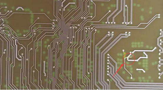
Circuit opens (or breaks) and shorts, as the name suggests, are unintended breaks in the circuitry of printed circuit boards. Depending on the location, these more often than not, have a significant impact on the functionality of the electronic device and may even cause serious damage to the board and the connected components.
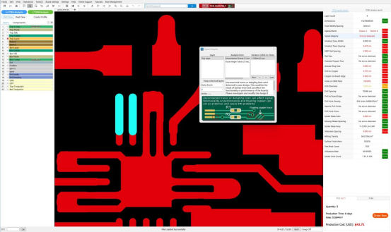
HQ Electronics' design analysis software HQDFM has the capability to detect circuit anomalies using the production files (Gerber or OBD++) with the IPC netlist file or purely by detecting the anomalies in the Gerber files.
During the design phase, shorts and opens may be introduced to the design by mistake or by not considering manufacturing limits.
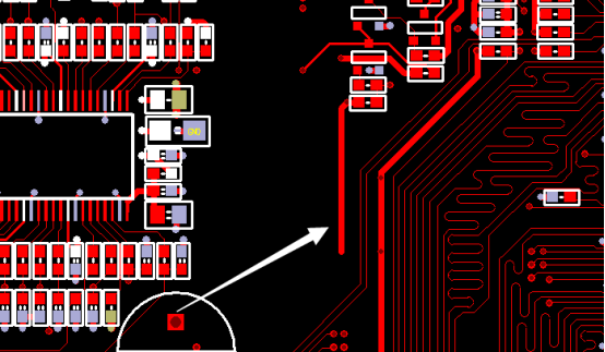
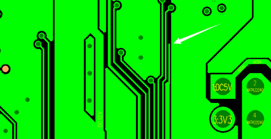
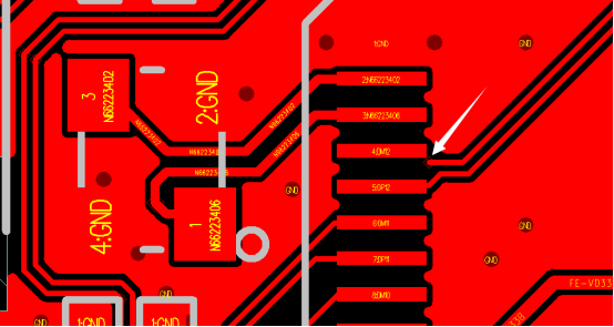
1. Opens may be the result of incomplete connections to pads perhaps from oversight during the routing process or intentionally left unconnected for to satisfy certain configurations.
HQDFM’s algorithms can easily detect such long, unconnected single-ended traces in the copper layers with or without the IPC netlist file and highlight them for review.
2. Narrow areas of copper pour due to poor copper optimization, while typically not as severe, may be mistaken for open unconnected traces and may make manual inspection more difficult. In high-speed designs, areas of floating copper may not be desirable in maintaining signal integrity.
HQDFM can detect such trace-like objects and they can be removed by configuring the copper pour settings in the design software or ignored if the effects are negligible.
3. When routing many traces under pressure, it is easy to imagine a simple twitch of the mouse pulling the trace away from the intended pad, resulting in an open. The mistake may not be obvious from lower zoom levels and the lack of efficient object snapping in the design software may make this kind of problem more prevalent and difficult to detect visually.
DRC netlist checks and HQDFM are very efficient at detecting such problems and it is advised to carry out both checks if available. Likewise, DRC and DFM checks are able to detect unintended shorts by comparing copper placement against the netlist.
Even after you have performed DRC and DFM checks, unintended shorts and opens may be introduced after you hand the production files off to your manufacturer. With a reliable manufacturer, these will be handled and repaired internally so the designer usually does not have to worry. In the event shorts or opens do occur, the frequency of occurrence and understanding how circuit errors are introduced in the manufacture of PCBs can help determine the source of the error and measures that can be taken to avoid them.
1. Shorts can be introduced in the creation of etching films and etching and plating processes. If etching films are not produced accordingly, all the boards produced with this film will share the same defects. If etching and plating are not uniform, some defects may only affect a small portion of the boards.
2. In a previous example, we looked at long unconnected traces that may have been intentionally left unconnected by the designer. Such long unconnected traces also pose a production risk, as it is easy for them to detach from the PCB substrate and reattach in other areas, causing shorts. While this defect can be detected in subsequent automated inspection processes and fixed in simple cases, widespread defects may not be salvageable and could have a significant impact on yield.
3. As copper features and spacings shrink and approach the manufacturing limits of the board fabricator, more and more random defects will occur as plating and etching processes become harder to control. Unless where necessary, encroaching the limits of the manufacturer should be kept to a minimum to maximize the number of defect-free boards. Otherwise, another production run may be necessary to produce enough boards required by the customer, which of course incurs additional delays and costs.
For example, 3.5mil trace widths are a challenge for many fabricators but are required by fine-pitch BGA fan-out designs. Fabricators can achieve this if the design keeps 3.5mil traces to a minimum, i.e. only where the trace runs between BGA pads, and by producing more excess boards in the hope enough will pass specifications.
Likewise, even if a fabricator’s specification mentions 4mil traces as their minimum, it is not desirable to make all traces 4mil if the current carrying capacity allows and when wider traces are also acceptable.
HQDFM considers the manufacturing limits of PCB fabricators in the wider industry in addition to HQ Electronics and will highlight board features that are pushing the limits and give suggestions to improve manufacturability and yield, and therefore reduce unnecessary costs and delays
HQDFM software provides a one-click analysis of circuit opens and other design issues, intercepting them before manufacturing, thereby avoiding the need to address and communicate problems after design handoff, which would significantly waste time.
Detection of opens using Gerber file elements
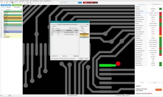
Detection of opens using the IPC netlist
If issues are not detected during PCB fabrication and the product is populated with parts, only to discover that the product is non-functional, would result in not only the lost cost of the PCB but also component costs.
By analyzing and checking design files in advance using tools like HQDFM, reliability issues can be prevented, production cycles can be shortened, product quality can be improved, and research and development costs can be reduced. Download HQDFM for free today or try the online Gerber Viewer for a quick trial.
Still, need help? Contact Us: support@nextpcb.com
Need a PCB or PCBA quote? Quote now


 Surface

