NextPCB Capabilities
Printed Circuit Boards
NextPCB Capabilities
Printed Circuit Boards
 PCB Assembly
 Layer Buildup
 SMD-Stencils
 PCB Design-Aid & Layout
 Mechanics
 Quality
 Drills & Throughplating
 Factory & Certificate
 PCB Assembly Factory Show
Certificate
PCB Assembly Factory Show
Certificate
Support Team
Feedback:
support@nextpcb.com


Your PCB design looks perfect in KiCad; you’ve gone through all the ERC and DRC warnings, double-checked every pin and you’re ready to get these printed circuit boards printed, but what’s that? The manufacturer is asking for Gerber files? What’s a Gerber file? Why can’t you just hand them the KiCad design? Why are there so many settings? What will happen if you get one of these wrong? Is it Gerber as in Gerbil? Or Gerber as in Gertrude?
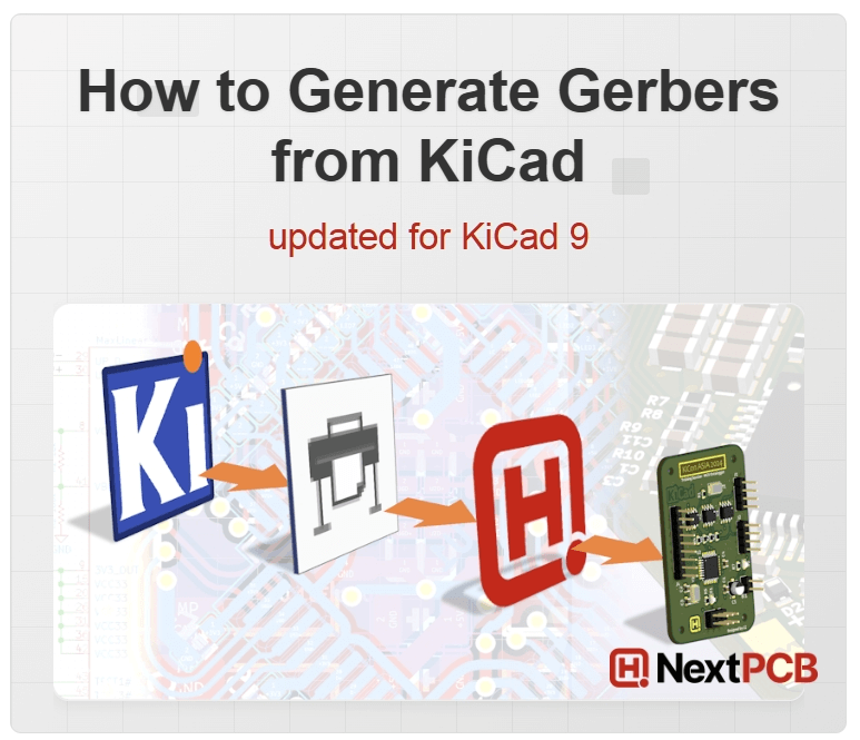
This article will cover how to generate Gerber files in KiCad, answer all the questions above and more; including common pitfalls and tips to get your PCBs manufactured right the first time.
This guide has been updated to KiCad 10 (KiCad 10.0.5 to be precise). Screenshots with the black UI are from KiCad 10, which introduced official support for dark mode.
If you just need a quick template to copy the settings, refer to our quick Gerber guide here.
Gerber files (pronounced with a hard G) are the de facto industry standard file format for transferring PCB manufacturing data. If someone wants to get a PCB board fabricated, more likely than not, they need to export Gerber files from whatever tool they are using. Be it KiCad, Eagle, Altium, Zuken or Target9001, just about every modern EDA tool supports Gerber file export natively, even if it is deliberately restricted or behind a paywall. A manufacturer that supports native KiCad files is likely just taking care of the Gerber export for you, which helps reduce errors.
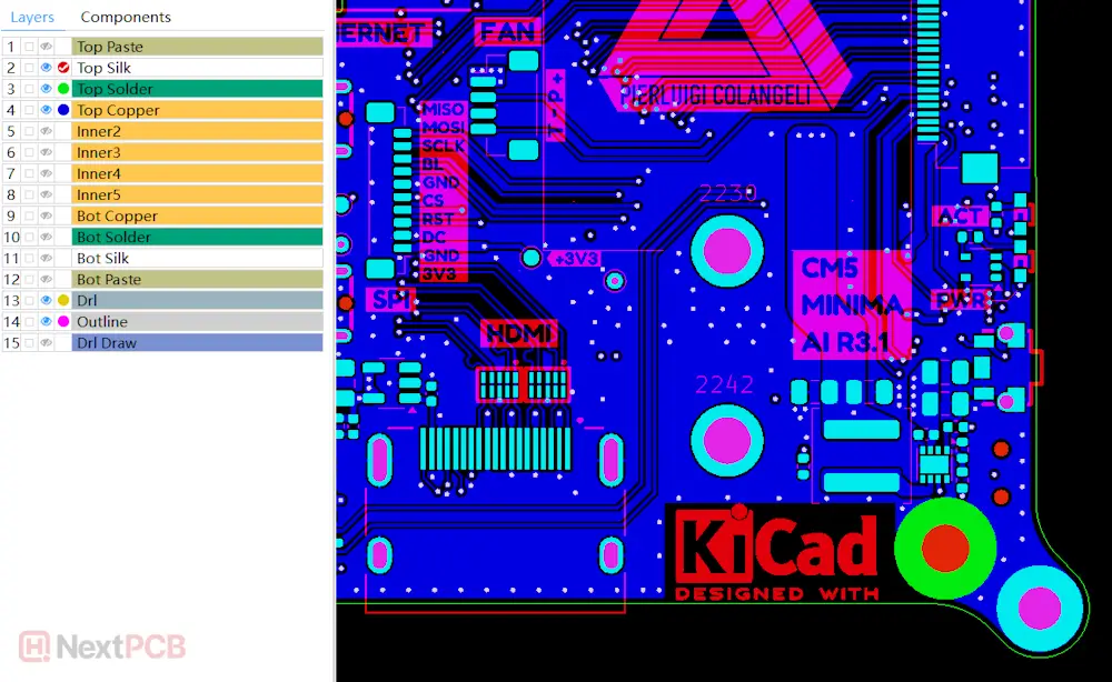
Pierluigi's CM5 MINIMA design Gerber files as they appear in HQDFM free DFM tool
Other file formats exist that attempt to address Gerber's limitations, such as IPC-2581 and ODB++, but both EDA tool support and fabricator adoption remain limited, and neither format is nearly as mature as Ucamco's Gerber specification.
But even within the Gerber specification, there are different formats.
RS-274X Gerber: You will most likely hear about Gerber files in RS-274X format (otherwise known as X1 or Extended Gerber), which is the most commonly accepted.
X2 and X3 Gerber: Newer X2 and X3 formats have more information appended, such as stack-up and component placement. However, this information may not be utilized by the manufacturer and may have compatibility issues with older software.
RS-274D Gerber: RS-274D is the predecessor to RS-274X and is now almost obsolete. This format is highly prone to errors and compatibility issues. Not recommended for new designs!
If in doubt, check with your manufacturer or export in RS-274X format.
Manufacturers and designers alike will refer to PCB production data as “Gerber files” or just “Gerbers.” In reality, they are referring to Gerber files + drill files + any other production documentation, such as stack-up and impedance control information.
Likewise, a single PCB design is represented by several individual Gerber files, not ‘a single Gerber file,’ depending on the number of layers and sides. In KiCad, each KiCad layer translates to a Gerber file when exported. Manufacturers, especially those with online ordering systems, often ask for all the PCB production data to be packaged into an archive file e.g. .zip or .rar for easy handling.
Don’t forget the drill file!
The drill file is technically not in Gerber format, but it is just as important. In KiCad, the drill file export process is another step separate from Gerber generation, which can make it easy to forget. Worst-case scenario, your board gets manufactured without any drill holes!
Both Gerber and drill files are ASCII text files containing coordinates and basic plotting commands that 'draw' the monochromatic manufacturing layers, such as copper, solder mask, silkscreen and outline. To visualize Gerber files, you'll need a specialized viewer, like NextPCB's free online Gerber Viewer.
For more detailed information on the individual Gerber layers and the information they contain, you can read our 3-part article series on All About Circuits here.
The basic Gerber export process itself is very simple. Once you have the configuration settings for your manufacturer set up, it only takes 4 clicks to export the PCB Gerber files and drill files:
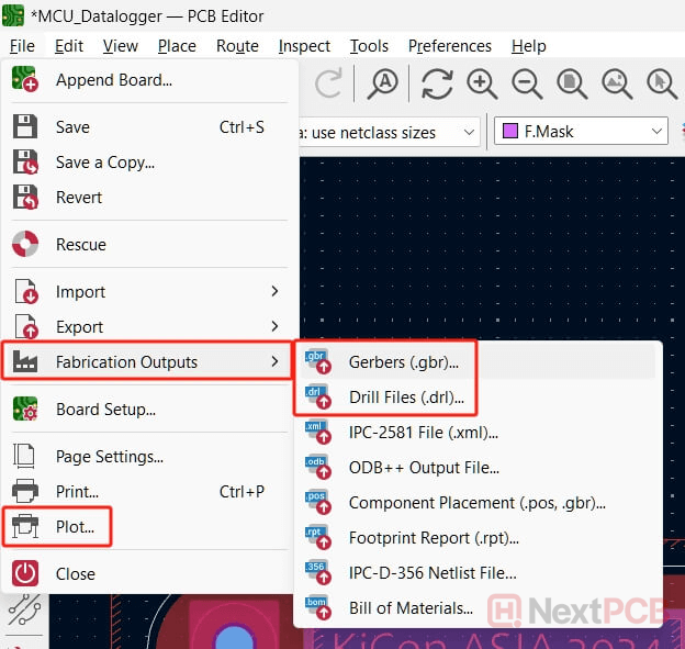
Now your Gerber and drill files have been exported to the output directory.
That was easy, right? However, knowing how to set up the configuration to suit both your design and supplier is another problem altogether, and can be daunting for the beginner and even seasoned KiCad users. In fact, many options are to maintain compatibility with older systems or only apply to niche situations like making DIY PCBs at home. The KiCad team has made export simpler over the years and regularly makes adjustments based on user feedback.
Since export settings are saved with the design file, default settings essentially don't exist. Therefore, having a basic familiarity with each setting and its impact gives you control and peace of mind, whatever project you are working on.
Let’s go into each option in detail:
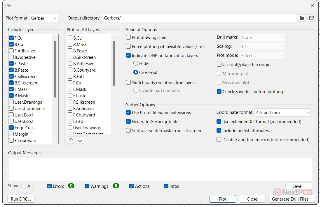
KiCad 9's export interface remains largely untouched in KiCad 10, with only some positions changed and the removal of plotting invisible values
Plot Format: The default is Gerber format, but KiCad supports plotting to many other formats, including SVG, Postscript, DXF, and even PDF for outlines and importing into other software. For production, we will need the output in Gerber format.
Output Directory: This is the directory where KiCad will dump the exported Gerber files. The default value is the original directory in a new folder named Gerbers. You can open the output directory directly by clicking the button on the right.
Include Layers: This section allows you to select the KiCad layers to export as Gerber files. One Gerber file is generated per selected KiCad layer. However, not all of these are necessary for production. The layer names in the screenshot may differ from your design settings and KiCad version, but generally the following Gerber layers are needed for a two-layer PCB design:
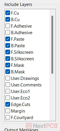
The layers needed for production include the copper, solder mask, silkscreen and outline layers.
The paste layers are required for surface mount designs if you intend to make a PCB stencil for assembly. Even if you don’t need stencils, including them does not hurt. If your design consists only of through-hole components, the paste layers will be empty for obvious reasons.
For multilayer designs, be sure the inner copper layers are selected. If you have vital information in other layers you need to pass on to the manufacturer, be sure to export these layers as well.
Plot on All Layers: This section allows you to copy the contents of a layer to all other layers. For example, you may want to copy the board outline in the Edge.Cuts layer to other layers for alignment. Be careful with this, however. Accidentally copying silkscreen or traces to all your layers could completely ruin the other Gerber files and cause short circuits.
Many of the General Options apply to PDF exports or fab Gerber layers that are used for assembly. The only option relevant to bare PCB manufacture is the Check zone fills before plotting option. Unless you have custom zone fills you need to preserve, checking this is good practice and can save you a lot of trouble.
Plot drawing sheet: This plots the PCB editor's page frame and title block to all of your exported Gerber files. This can be good for housekeeping and differentiating between different versions. Just keep in mind that - since it is exported to the outline Gerber layer, it can interfere with automated dimension detection and some 3D PCB viewers. When using automated order forms for quotes, make sure the detected board size matches your actual PCB - not the 190 by 128mm frame.
Feel free to leave the following options unselected for basic PCB manufacture:
Force plotting of invisible values/refs (removed in KiCad 10): As the name suggests, this option plots values and references that are hidden/invisible in the PCB editor. Use with caution.
Sketch pads on fabrication layers: This option adds the outlines of all the pads onto the fabrication layers. This can be useful for quickly finding components that don't have outlines in the fab layers, especially when viewed without other Gerber layers. But it can also clutter a fab layer and make designator labels hard to read. Including pad numbers can clutter even more for small parts.
Use drill/place file origin: This forces Gerber files to use the custom origin set using the Drill/Place File Origin tool, also known as the auxiliary origin. When enabled, the matching setting in the drill file export dialog is also selected. Feel free to use this option if required, so long as the origin is consistent across all files.
KiCad 10 Changes:
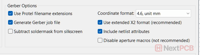
Use Protel filename extensions: This option applies the Protel-style extensions (.GTL, .GBL, .GTO, .GBO) to the exported Gerber files instead of the generic .gbr suffix. The original filename and file format do not change; they simply serve as labels for identification. The KiCad pop-up says this is no longer recommended, however, some automated Gerber file readers (e.g. Gerber Viewers) rely on this as a foolproof way to reliably identify and auto-assign layers. Because the Protel naming scheme is widely recognised even in non-English-speaking countries, using these extensions can improve communication and consistency.
Generate Gerber job file: This is a non-production file that logs the files exported. It is not necessary, but can add some insights into the design, such as the version of KiCad used - useful when investigating version-specific issues.
Subtract soldermask from silkscreen: This option removes sections of silkscreen where there are solder mask openings (areas with no solder mask). This is typically to prevent silkscreen from being printed onto copper pads and interfering with soldering - however, most fab houses already do this subtraction when processing your files. You can use this option if you’d like to preview the result of subtraction or if you know the manufacturer does not offer this service.
Coordinate format: KiCad only offers two coordinate formats (other EDA tools have more customization), and either one will likely not affect your boards in any way. The only difference is the number of digits after the decimal point, which indicates precision, where 6 decimals is more precise than 5. For high-speed and RF designs, submicron tolerances may be affected by rounding and could benefit from the higher precision.
Lower precision could be favorable for larger file sizes, where precision is not important, such as for PCB art. Large file sizes can crash CAD tools.
For this PCB ruler, with moderate graphical elements, the package does reduce in size, but only by about half an MB
Use extended X2 format (recommended): Check this feature to add X2 header attributes to the Gerber files, effectively changing the Gerber format from RS-274X to X2. It is recommended, however, though increasingly rare, some older manufacturers do not accept X2 Gerber files.
Include netlist attributes: This adds netlist-like attributes to the Gerber files that can be utilized by some CAD tools.
Disable aperture macros (not recommended): Aperture macros offer support for complex geometric shapes and can reduce file size. However, like Gerber X2 attributes, aperture macros can cause compatibility issues with older software. These errors can be difficult to detect because they only affect these macro- based apertures, like a hexagonal pad or thermal, for example. Older, unmaintained Gerber viewers are known to render these features incorrectly.
Clicking the Generate Drill Files button will bring you to the drill file export dialog. Simply click the Generate button to plot the drill file in the output folder.
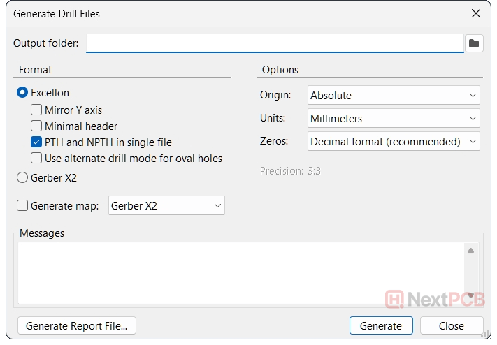
Format: Drill files are often requested in Excellon format rather than Gerber, though KiCad supports X2 Gerber export as well.
PTH and NPTH in single file: The pop-up says this is not recommended, but manufacturer preferences vary. In practice, many accept both merged and separate options. The advantage of having them merged is that you are less likely to leave one out and end up with missing holes.
Options: KiCad offers much more format customization for drill files
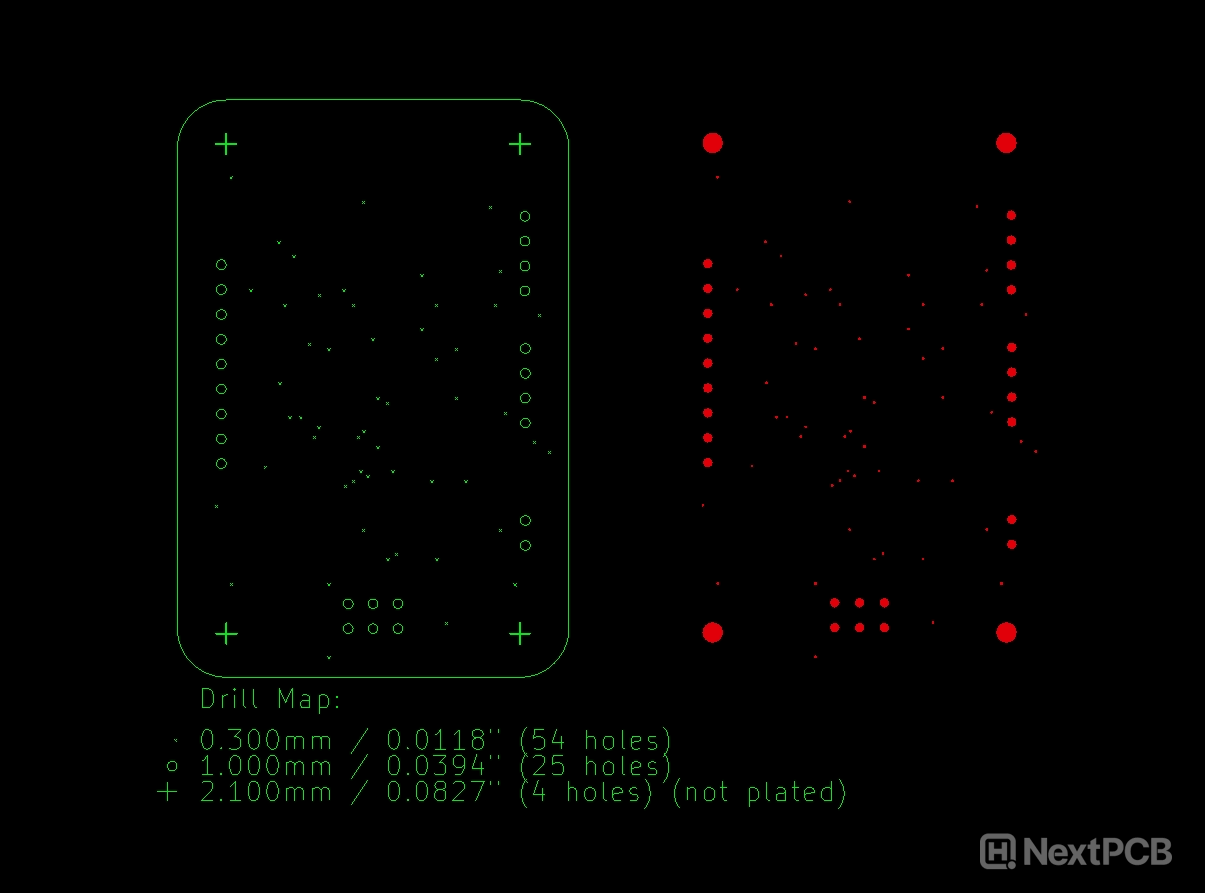
Generate Drill Map: KiCad provides the option to export the drill map. This is a Gerber layer that provides location and size information graphically rather than literally. Unlike Excellon drill files, drill maps can contain extra information such as the nature of the drill holes, the quantity and size in written word. However, Excellon drill format files are more widely accepted compared to drill maps, and typically a manufacturer that can handle drill maps will also accept Excelllon drill files, but manufacturers that ask for Excellon drill files will not necessarily accept drill maps, as it may require additional manual input.
Compare drill maps to Excellon drill files on the right:
The above suggestions are generic and should apply to the large majority of PCB fab houses. However, some have individual preferences that work best for their software and equipment. Always follow the manufacturer’s recommended guidelines first.
On that note, however, if you have already handed over your files and later realize you didn't follow the recommended format, it's generally nothing to worry about. Modern CAM tools and workflows can accept a wide range of formats or have ways to deal with them - sometimes just changing the import settings. The data is not wrong - it just needs another way to interpret it. 9 times out of 10, the manufacturer-provided Gerber export guide is there to make sure 1) you export Gerber + drill files and 2) don't omit any necessary files.
Still don’t know what works best for your design and fab? Thanks to KiCad’s open-source nature, support for KiCad files is widely available. Some manufacturers accept native KiCad files or have tools for exporting the files to their recommendations, so you can skip the Gerber file export nonsense altogether.
Numerous manufacturers have developed their own KiCad plugins to support Gerber export and even send the output files to their website directly. The settings are pre-configured to their preferences for optimal compatibility.
Manufacturers with native KiCad file support take .kicad_pcb files directly and take care of Gerber export.
NextPCB has a mixed approach, with KiCad plugins and a direct Gerber export service.
Before you go to production, make sure you check these important things off your list!
Understand your chosen manufacturer’s requirements: Check the website for information regarding their manufacturing capabilities, accepted files and other services. They may have specific guides for exporting Gerber files from KiCad, KiCad plugins or direct KiCad file support.
Check your Gerber files!: When you export Gerbers from KiCad, your design is being translated from KiCad’s native format into the standardized Gerber/Excellon formats used by PCB manufacturers. Like any translation, errors can and do occur. Missing layers, traces, solder mask openings -- these mistakes are costly if left undiscovered but are easily discovered in a Gerber Viewer. KiCad has a simple Gerber Viewer tool built-in so there are no excuses. Don’t let all your hard work go to waste.
Perform DFM Analysis on the Gerber Files: Going a step further, you can perform Design for Manufacture and Assembly analysis (DFMA) on the PCB Gerber files with specialist tools such as HQDFM by NextPCB. HQDFM is a free PCB design analysis tool with DFM and DFA analysis capabilities that checks over 1200 detailed inspection items that go beyond DRC checks to reduce manufacturing errors, improve reliability and reduce costs. HQDFM also serves as an advanced Gerber viewer with helpful production tools including a Gerber panelizer, impedance calculator, footprint checker and more.
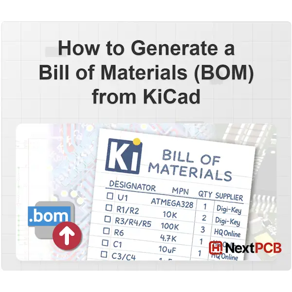
Double, triple check your footprints and Bill of Materials: Now that you have the PCB design covered, be sure to check the assembly documentation:
HQDFM has free tools for automating these tedious actions, including a footprint checker covering over 6 million parts and a BOM file checker.
Check your design in KiCad’s 3D viewer: Make use of KiCad’s 3D viewer during the design phase. It updates in real-time, so you can get immediate feedback as you complete your design. For Gerber files, HQDFM has a realistic viewer and 3D viewer as well.
>> Advanced Design Note
Are you designing for 6G modules, AI edge devices, or miniaturized sensors? Your KiCad export settings could be the bottleneck. Check out our technical deep-dive: Gerber File Precision for UHDI PCBs: Beyond the 2:4 Standard


NextPCB provides PCB manufacturing and assembly services, focusing on reliability without breaking the bank. With 5 factories in China and over a decade of quick turnaround electronics manufacturing from prototype to mass production, NextPCB serves over 160 countries around the world, pairing dependable electronics hardware with exceptional service.
As a Platinum KiCad sponsor and long-term supporter of the KiCad open-source ecosystem, NextPCB's contribution spans developer funding, and hosting KiCon Asia — the largest KiCad‑focused event in the region. This KiCad Hub brings together all of our tutorials, tools, projects, and community contributions into one place, making it easier for designers of all levels to learn, explore, and build with KiCad.

Still, need help? Contact Us: support@nextpcb.com
Need a PCB or PCBA quote? Quote now


 Surface