
 Surface


Stacy Lu

 NextPCB Capabilities
Printed Circuit Boards
NextPCB Capabilities
Printed Circuit Boards
 PCB Assembly
 Layer Buildup
 SMD-Stencils
 PCB Design-Aid & Layout
 Mechanics
 Quality
 Drills & Throughplating
 Factory & Certificate
 PCB Assembly Factory Show
Certificate
PCB Assembly Factory Show
Certificate
Support Team
Feedback:
support@nextpcb.com


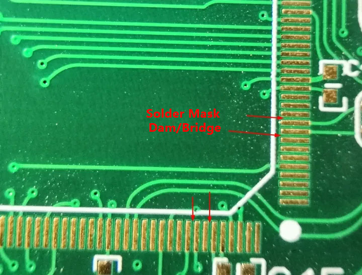
A solder mask bridge, also known as a solder mask dam, or sometimes referred to as a "solder resistance bridge" or "dam PCB" , is a small section of the solder mask layer on a printed circuit board that is left open or exposed around the perimeter of each pad or through-hole. The purpose of a solder mask bridge is to prevent the flow of solder or other conductive materials from one electrical connection to another during the assembly process.
Contents:
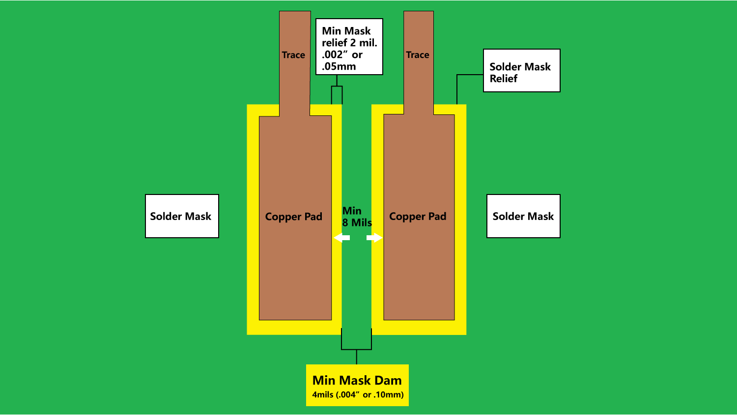
By creating a small barrier, the solder mask dam ensures that the solder joints are formed only where intended, preventing electrical shorts and other types of damage that can cause electronic devices to malfunction or fail. Solder mask dams are important for ensuring the reliability and performance of electronic devices, as they protect the copper traces and other metal features from oxidation, contamination, and other forms of damage.
Solder mask is a complex mixture primarily composed of resin (such as epoxy, polyurethane, or acrylic), hardener, fillers, dyes, and UV-reactive substances. The choice of solder mask material is crucial:
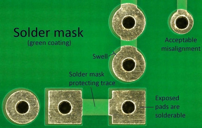
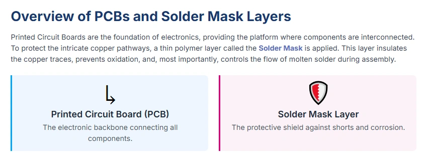
Printed circuit boards are the backbone of many electronic devices, providing a platform for electronic components to be connected and communicate with each other. The solder mask layer is a thin, uniform layer of polymer material that is applied to the surface of the board to protect the copper traces and other metal features from oxidation, contamination, and other forms of damage. The solder mask layer also serves as a barrier to prevent the flow of solder or other conductive materials from one electrical connection to another.
Solder mask dams are an essential feature of the solder mask layer. By creating a small barrier around each pad or through-hole, solder mask dams prevent the flow of solder outside of the intended area during the assembly process. This ensures that the solder joints are formed only where intended, preventing electrical shorts and other types of damage that can cause electronic devices to malfunction or fail.

Solder mask dams are particularly critical for:
Solder mask dams function by preventing the solder from flowing outside of the intended area during the assembly process. Without solder mask dams, molten solder can flow onto adjacent conductive features, causing electrical shorts (solder bridges) or other types of damage.
During fabrication, the solder mask is applied over the entire board and then selectively removed from areas where soldering is required (pads, vias). The dam is the intentional, intact strip of solder mask material left between two closely spaced pads or pins. By acting as a physical "dam," this strip ensures the surface tension of the molten solder confines it to the intended pad, improving the reliability and quality of the PCB assembly. Solder mask dams are crucial for preventing these types of problems and ensuring the reliability and performance of electronic devices.
There are several types of solder mask dams that can be used, including open, hatched, and round dams. Each type of solder mask dam has its advantages and disadvantages, and the appropriate type should be selected based on the specific requirements of the PCB design.
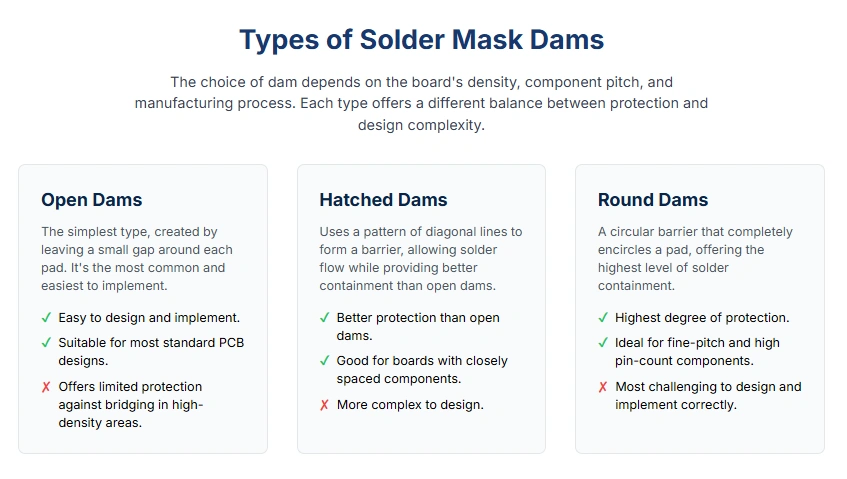
Open solder mask dams are the simplest and most common type of solder mask dam. They are created by leaving a small open space around each pad or through-hole, allowing solder to flow onto the pad or through-hole without spreading to adjacent conductive features.
| Advantages | Disadvantages |
| Easy to design and implement | Limited protection against solder bridging or other types of damage |
| Suitable for most PCB designs | May not be suitable for designs with closely spaced components or high-density PCBs |
| Can be used with most soldering techniques |
Hatched solder mask dams are similar to open solder mask dams, but they use a pattern of diagonal lines to create a barrier around each pad or through-hole. The diagonal lines create small gaps in the solder mask, which allow the solder to flow onto the pad or through-hole without spreading to adjacent conductive features.
| Advantages | Disadvantages |
| Provides better protection against solder bridging or other types of damage than open solder mask dams | More complex to design and implement than open solder mask dams |
| Can be used with most soldering techniques | May not be suitable for designs with very fine pitch components or high pin-count devices |
| Suitable for designs with closely spaced components or high-density PCBs |
Round solder mask dams use a circular shape to encircle each pad or through-hole. The circular shape creates a barrier around the pad or through-hole, preventing solder from flowing onto adjacent conductive features.
| Advantages | Disadvantages |
| Provides the highest degree of protection against solder bridging or other types of damage | More challenging to design and implement than open or hatched solder mask dams |
| Suitable for designs with fine-pitch components or high pin-count devices | May not be suitable for designs with very closely spaced components or high-density PCBs |
| Can be used with most soldering techniques |

The way a pad is defined relative to the solder mask is a critical design decision directly impacting dam performance and assembly reliability.
| Feature | Solder Mask Defined (SMD) Pads | Non-Solder Mask Defined (NSMD) Pads |
| Definition | Solder mask opening is smaller than the copper pad. The mask covers part of the copper. | Solder mask opening is larger than the copper pad. The copper is fully exposed. |
| Solder Joint | Joint strength depends on adhesion to the top of the copper pad. | Solder wets all sides of the copper pad, forming a strong fillet. |
| Mechanical Strength | Higher mechanical strength, as the solder mask provides a physical anchor on the copper pad. Often used on flex PCBs. | Lower mechanical strength; relies solely on copper adhesion, increasing the risk of pad lifting, especially on large BGAs. |
| Bridging/Pitch | Preferred for very fine-pitch components (e.g., 0201/01005) as it minimizes solder bridging. | Less prone to solder voids because gas can escape easily during reflow. |
| Tolerance | Requires precise alignment between copper and mask; less forgiving of registration errors. | More forgiving of fabrication tolerances and misregistration. |
NSMD is generally preferred for large components and BGAs where high solder joint reliability is paramount, while SMD is often chosen for ultra-fine-pitch designs where preventing solder bridging is the top priority. However, it is important to note that the copper etching process is generally capable of a tighter tolerance than the solder masking process, leading to a general preference for NSMD pads.
Designing an effective solder mask dam requires careful attention to material properties, dimensions, and manufacturing tolerances.
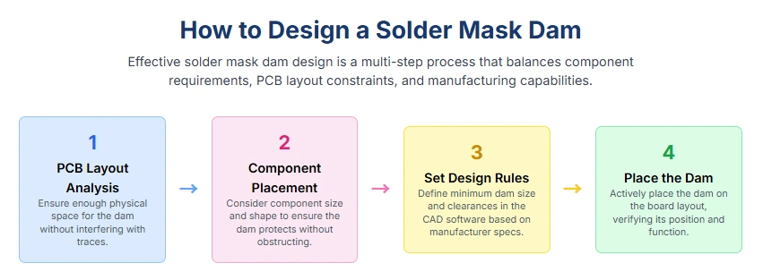
The PCB layout is an essential consideration when designing the SMD. The designer must ensure that there is enough space for the dam and that it doesn't interfere with other components or traces on the board.
Additionally, the placement of the components on the board is also important when designing the solder mask dam. The designer must consider size and shape and protect the component without obstruction.
The type of solder mask material used is also a significant consideration. The designer needs a compatible material for insulation and protection that fits the manufacturing process.
The first step in designing an SMD is to set up the design rules. We determine the minimum size and clearance for the dam and actively avoid any interference it may have with other components or traces on the board.
After setting up the design rules, the designer can actively begin placing the solder mask dam on the board. We must place the dam adequately to protect the component while ensuring it functions properly.
LDI technology has largely replaced traditional phototooling for high-accuracy solder mask application.
While tighter tolerances (such as narrower dam widths or more precise registration) improve performance, they inherently impact the fabrication process:
> Recommend reading: Custom PCB and PCBA Cost Analysis: How to Optimize Design and Reduce Expenses
In short, it is significant in making PCBs for electronic devices. Additionally, it also adds a layer of protection by covering the copper traces to prevent any accidental short circuits. Furthermore, this protective layer also prevents oxidation and corrosion.
> Recommend reading: IPC-2581: The Unified Data Standard for Smart PCB Manufacturing
It's part of the PCB fabrication process that involves several steps, including designing the PCB layout, printing the solder mask layer, and curing it. The solder mask's thickness, color, and material type affect the PCB's performance. It is significant to consider these factors when designing the solder mask layer. Proper design rule implementation, including the selection of appropriate dam widths and pad types (SMD vs. NSMD), is essential to leverage the full benefit of this critical PCB feature.

Still, need help? Contact Us: support@nextpcb.com
Need a PCB or PCBA quote? Quote now

