

 NextPCB Capabilities
 PCB Assembly
 Layer Buildup
 SMD-Stencils
 PCB Design-Aid & Layout
 Mechanics
 Surface
 Quality
 Drills & Throughplating
 Factory & Certificate


Introduction:
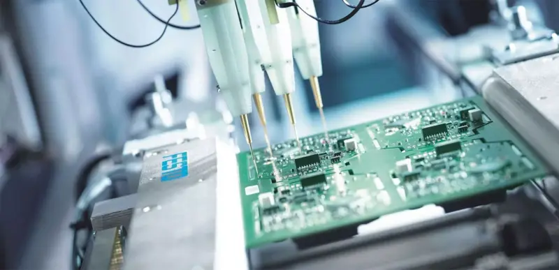
ICT (In-Circuit Test), an automated electrical structural testing method, is essential for modern PCBA mass production. It detects opens, shorts, component faults, and assembly defects on PCBAs by contacting test points exposed in the layout with test probes. The system pinpoints fault locations explicitly, enabling even operators with basic electronics skills to efficiently troubleshoot defective boards. ICT testing significantly boosts production efficiency, pcba manufacturing quality, and reduces manufacturing costs.
> PCB/PCBA Test Methods by Category
1. What is ICT?
ICT testing, one of the most popular pcb testing methods, is a methodology that uses electrical measurements via probes contacting test points on a PCB to inspect component values and connection integrity. It identifies soldering defects, component parametric deviations, shorts, opens, and incorrect part placement/orientation.
PCBs must incorporate dedicated test pads at strategic nodes. ICT equipment uses probes (arranged in a bed-of-nails fixture) to simultaneously contact these pads, connecting them to specialized test hardware. Measurements (powered or unpowered) rapidly identify assembly flaws: shorts, opens, incorrect R/C/L values, polarity errors, etc. This constitutes "white-box" structural testing, contrasting with visual-only AOI (Automated Optical Inspection) by measuring electrical parameters directly.
For high-density boards with limited test access, IEEE 1149.1 boundary scan (JTAG) can be integrated with ICT to enhance interconnect testing and programmability.
2. Explanation of Fundamental ICT Testing Principles
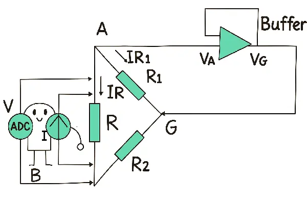
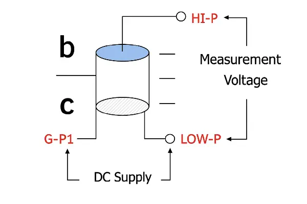
2.1 Guarding Principle
Guarding is fundamental to ICT. It isolates the component under test (CUT) from parallel circuit paths using a low-impedance buffer to force a "guard node" to the same potential as the test node (VG=VA). This diverts leakage currents (IR₁≈0), ensuring the measured current (I) flows only through the CUT. Thus, R = V/I accurately, unaffected by parallel resistances (R₁, R₂). The ICT system automatically selects optimal guard points based on test programming.
> HQDFM Gerber Viewer + DFM Pre-Check (test-point/spacing validation)
2.2 Resistance Measurement Methods
Constant-Current Method: Applies fixed current (I), measures voltage (V), calculates R=V/I. Requires sufficient source compliance voltage and settling time for RC networks; parallel capacitors/diodes can cause under-reading if unstable.
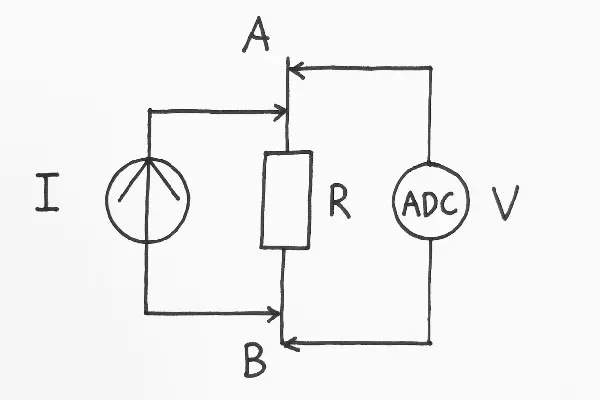
Constant-Voltage Method: Applies fixed voltage (V), measures current (I). Preferred when large parallel capacitors cause long charge times with constant-current method. Optimizing source resistance and sampling windows enables fast readings before full capacitor charging.
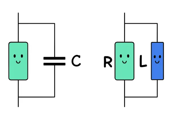
Phase-Sensitive Measurement: Used for resistors paralleled with capacitors or inductors. Applies AC constant-voltage signal, measures voltage-current phase difference (φ). Calculates impedance |Z|=V/I, resistance R=|Z|cosφ, and reactance X=|Z|sinφ (Xc or XL). Frequency is chosen to maximize resolution (when |X| ≈ R).
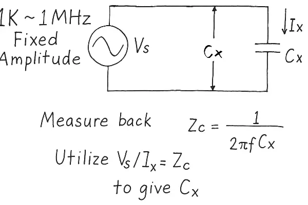
2.3 Capacitance Testing
AC Constant-Voltage Method: Ideal for small caps. Applies constant-amplitude sine wave at varying frequencies (f), measures resulting current (I). Calculates C ≈ I/(2πfV). Loss tangent (tanδ) can be estimated via multi-frequency measurement.
DC Constant-Current Method: Used for large capacitors (>1µF). Charges cap with fixed current, calculates C = I * Δt / ΔV. Requires limiting voltage step/charge time and compensating for leakage current.

Phase-Sensitive Method: For capacitors parallel with resistors. Provides C and Equivalent Parallel Resistance (EPR) to identify leakage/aging, similar to resistance measurement.
> FCT (Functional Testing) – validates functionality and complements ICT
2.4 Inductance Testing
Uses AC voltage source. Calculates L from measured current, voltage, and phase (L = |Z|sinφ / (2πf)). Higher frequencies are used for smaller inductances. Small signal levels prevent core saturation. Simple resistance checks can detect missing parts or solder opens.
> The Four Major Bare PCB Test Methods
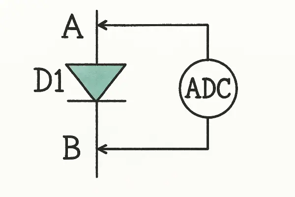
2.5 Diode Testing
Measures forward voltage drop (Vf) (typically 0.7V for Si, 0.2-0.4V for Schottky) with current limiting to identify opens, shorts, incorrect placement, or damage.
> X-Ray Inspection – reveals hidden solder joints and shorts in BGA/QFN packages
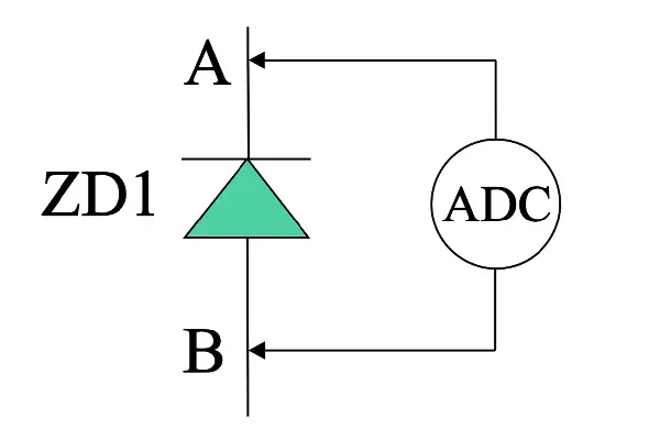
Zener Diode Breakdown Voltage (Vz): Uses ramped DC source with current limit to identify the knee voltage. Monitors power dissipation to prevent damage.
2.6 Transistor Testing
Two-Terminal Test: Measures B-E and B-C junction Vf (~0.7V). Deviations indicate shorts, opens, or reversed polarity.
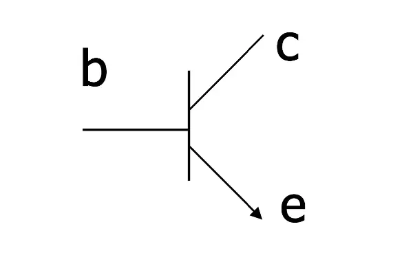
Three-Terminal Test: Applies base bias to saturate transistor, measures low VCE(sat) (~0.1-0.3V) between collector and emitter. Checks solder integrity and gain.
| Transistor Type | High-potential (HI) | Low-potential (LO) | Ground (G) |
|---|---|---|---|
| NPN | Collector (C) | Emitter (E) | Base (B) |
| PNP | Emitter (E) | Collector (C) | Base (B) |
2.7 Shorts/Opens Testing
Learn Phase: Measures resistance between all test point pairs on a known-good board. Points <10Ω (configurable threshold) are grouped into shorts groups (nets). Creates a "golden fingerprint" database, accounting for fixture contact resistance and board material.
> Alternative for low-volume: Flying-Probe Testing
Opens Test: Checks continuity between all test points within the same shorts group. A high resistance indicates an open.
Shorts Test: Checks resistance between points not in the same group and between groups. Resistance <10Ω indicates an unintended short. Fixture pressure adjustment or board flipping verifies marginal readings.
> Learn NextPCB's PCB Assembly Capabilities (end-to-end electrical test & process coverage)
2.8 Capacitor Polarity Test
Requires three probe points: Case (Top), Cathode (-), and Anode (+) as the guard. Applies voltage. Correct polarity yields low measured voltage due to charging. Reversed polarity or poor top contact yields high voltage. Low-energy pulses/current limiting protect parts and utilize ESR/leakage differences.
2.9 HP TestJet Technology
Standard diode tests fail on parallel IC pins or floating/flawed ESD structures.
HP TestJet Solution: A sensor plate on the fixture top matches the IC package. Measures capacitance between the plate and the IC's lead frame (~pF range). Open pins show a significant capacitance deviation from the learned profile.
> IC Programming (JTAG/ISP/ICP & boundary-scan interfaces)
> BGA Assembly Capabilities (AXI/AOI/boundary-scan synergy)

3. Limitations of ICT Testing
- Resistors in Parallel: R1 >> R2: R1 untestable. R2 >> R1: R2 untestable. Both R1 & R2 very small (e.g., <5Ω): Limited test accuracy.
- Capacitors in Parallel: C1 >> C2: C2 untestable (small cap obscured by large cap).
- Inductors/Jumpers in Parallel: L1 >> L2: L1 untestable. Jumpers parallel with inductors are untestable.
- Diode Parallel with Low-Value Resistor: R ≤ 10Ω limits test voltage to <1.0V (using max 100mA), insufficient for diode Vf test.
- Capacitor Parallel with Inductor (LC Tank): Capacitance cannot be isolated/tested.
- Small Capacitor Parallel with Low-Impedance Resistor: Small capacitor untestable.
- Large Capacitor Parallel with High-Impedance Resistor: Resistance untestable.
4. Advantages and Limitations of ICT Testing
Advantages:
- High Efficiency: Tests multiple parameters simultaneously.
- High Precision: Detects minute solder defects and component deviations.
- High Automation: Ideal for high-volume lines; minimizes manual effort/error.
Limitations:
- Physical Access Requirement: Probe contact necessitates exposed test pads; poor layout causes coverage gaps.
- Fixture Cost: Custom bed-of-nails fixtures are expensive; adaptability requires optimization.
- Limited Functional Test Scope: Not suitable for complex functional testing of large-scale integrated circuits.
> Functional Testing (FCT – complements ICT with system-level validation)
> Learn where ICT testing fits into the overall PCB manufacturing cycle: PCB Manufacturing Basics: Design, Fabrication, Testing, and Compliance
5. Applications and Future of ICT Testing
ICT testing is critical in consumer electronics, telecom, automotive electronics, and medical devices. Future trends driven by miniaturization and integration:
- Higher Integration & Miniaturization: ICT requires increased resolution/precision for high-density, fine-pitch boards.
- Multi-Functionality & Intelligence:
- Integration with optical inspection (AOI), thermal imaging, etc.
- AI and big data analytics for enhanced defect detection and root cause analysis.
- Increased Automation: Seamless integration into smart factories (automated loading/unloading) improves throughput and accuracy.
- Wireless/Non-Contact Methods: Development of contactless techniques for complex PCB designs increases flexibility.
- Programmable Testing: Adoption of programmable methodologies (leveraging FPGAs/MCUs) for adaptive test routines based on specific board requirements.
> PCB Assembly Capabilities (from SMT/THT through ICT/AOI/AXI/FCT)
> Free Functional Testing for Prototypes
Ready to Revolutionize Your PCBA Quality Control?
Unlock the full potential of ICT testing with precision-engineered solutions tailored to your manufacturing needs. Our experts deliver cutting-edge test fixtures, adaptive programming, and AI-driven analytics to slash defect rates by up to 90%.
Request a Custom Fixture Quote today to transform your production line!
> Get One-Stop PCB Assembly Ordering (Instant Quote)
> Free Functional Testing for Prototypes
> HQDFM Online DFM Analysis (one-click pre-order self-check)

