
 NextPCB Capabilities
Printed Circuit Boards
NextPCB Capabilities
Printed Circuit Boards
 PCB Assembly
 Layer Buildup
 SMD-Stencils
 PCB Design-Aid & Layout
 Mechanics
 Quality
 Drills & Throughplating
 Factory & Certificate
 PCB Assembly Factory Show
Certificate
PCB Assembly Factory Show
Certificate
Support Team
Feedback:
support@nextpcb.com


Compact IoT controllers now combine MCU, wireless, sensors and power management on very small PCBs. As board size shrinks, routing congestion, fine-pitch BGAs, dense power pins, and RF constraints quickly push traditional 2- or 4-layer designs to their limits.
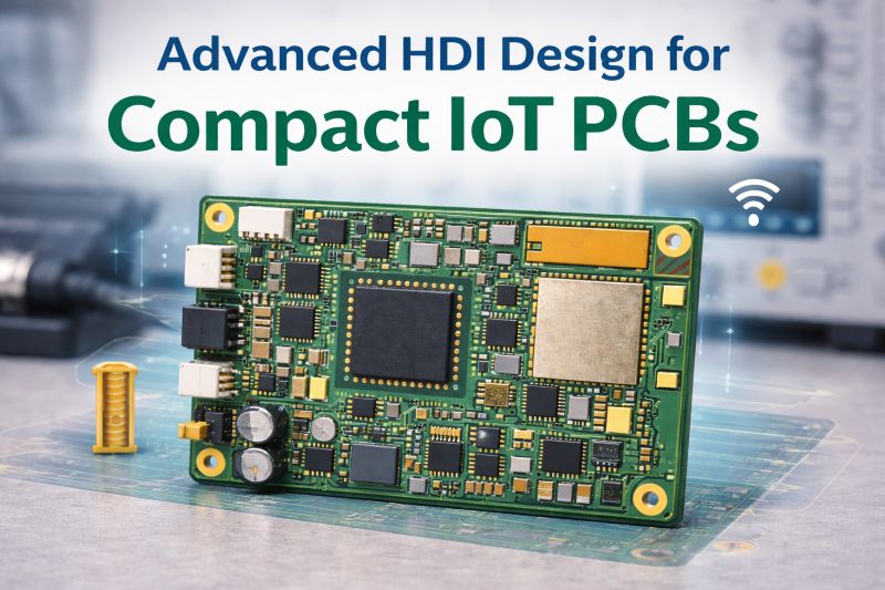
Compact HDI PCB integrating MCU, wireless module and power management in a space-constrained IoT design
HDI PCB technology solves these density challenges using microvias and optimized stackups to enable clean signal escape and stable power delivery. This article walks through a practical, step-by-step project showing how HDI turns a constrained IoT layout into a production-ready design.
In this project, we are designing a 50 mm × 40 mm compact IoT controller intended for industrial monitoring and smart infrastructure applications. The board must collect sensor data, process it locally and transmit it wirelessly — all within a single compact PCB.
We are not designing a simple sensor node. The board must integrate:
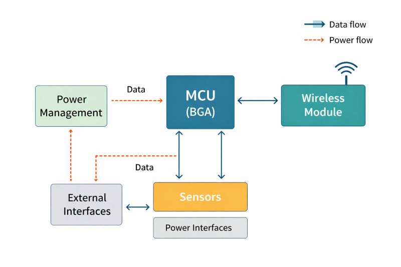
IoT Controller System Block Diagram: Functional architecture of the compact IoT controller before PCB layout begins
On a standard 4-layer board, routing under the MCU quickly becomes congested. Power pins cluster tightly. RF routing demands clean impedance control and antenna isolation. Simply adding layers increases cost but does not fix breakout congestion.
To make this board manufacturable and reliable, we will:
This project will walk through each of these decisions step by step — from constraints to placement, stackup, fanout, routing and DFM validation.
Before placing a single component, we lock the constraints. In compact IoT projects, most redesigns don’t happen because traces were routed badly — they happen because requirements weren’t fixed early.
For this controller, we define three hard boundaries: electrical, mechanical, and manufacturing.
This board must support:
These requirements immediately increase:
This tells us early: a simple multilayer board will likely struggle.
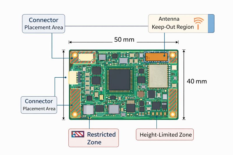
50x40mm IoT PCB Mechanical Constraints: Mechanical and placement constraints fixed before routing begins
The enclosure fixes the board size at 50 mm × 40 mm. Connectors and antenna position are pre-defined. Component height is limited.
We cannot:
This removes traditional layout escape options.
Once the project constraints were locked, the next major decision was stackup selection. In a compact 50 × 40 mm IoT controller, stackup determines whether BGA fanout will route cleanly, whether RF signals will maintain a stable reference, and whether power delivery will remain reliable during wireless transmission peaks.
Early evaluation showed that a 2-layer or standard 4-layer board could not support dense MCU breakout or controlled RF routing. Even a conventional 6-layer stackup struggled because through-hole vias consumed too much escape space under the fine-pitch package.
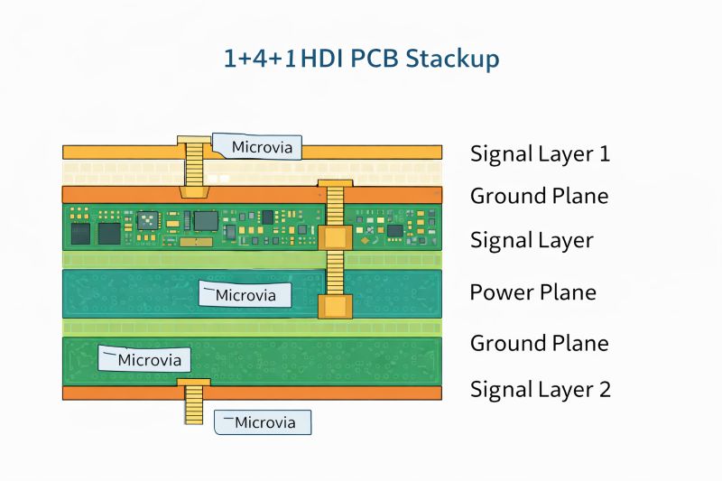
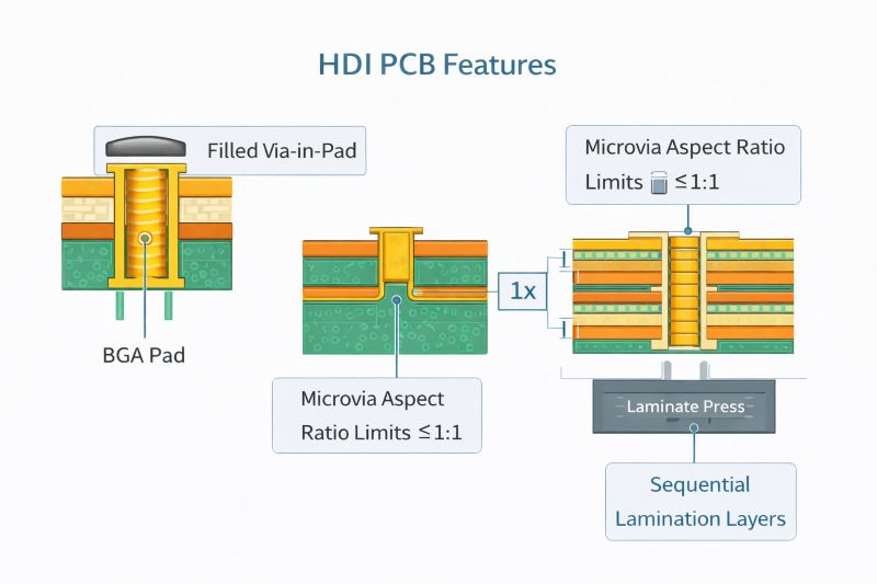
1+4+1 HDI PCB Stackup Structure: The 1+4+1 stackup enables clean BGA fanout and stable reference planes
Image File name - 1-4-1-hdi-pcb-stackup-structure
To solve this without over-engineering the board, the design adopted a 1+4+1 HDI stackup. This structure enables direct microvia fanout from the MCU, keeps signal layers tightly coupled to solid ground planes, supports low-inductance power delivery, and maintains mechanical symmetry for reliable assembly. Microvias are limited to adjacent layers only, with no stacking, keeping fabrication practical and scalable. The result is the simplest HDI configuration that eliminates routing congestion while remaining production-friendly.
In this project, we quickly realized that routing would not decide success—placement would. In compact IoT controllers, poor placement can increase layer count, force aggressive microvia usage, and create signal integrity problems that no routing trick can fix later. So before drawing a single trace, we treated placement as the most critical engineering step.
Insert Image 4 Here
Alternative Text - MCU centered placement with wireless module near edge and organized power section in HDI IoT PCB
Caption - Strategic placement reduces routing congestion before fanout begins
Image File name - hdi-iot-pcb-component-placement-strategy
The MCU was placed first and positioned near the center of the PCB. This provided balanced routing access on all four sides and allowed microvias to escape cleanly into adjacent layers. Placing it near the edge would have immediately restricted breakout channels and increased stackup complexity. The wireless module was locked early as well, positioned near the board edge with a defined antenna keep-out zone. This prevented RF compromises later and avoided the common mistake of trying to fix antenna performance during routing.
Sensors and interfaces were grouped logically based on signal flow rather than convenience. Devices communicating directly with the MCU were kept physically close to reduce trace length and noise exposure. The power section was placed with current flow in mind—regulators close to their loads, decoupling capacitors directly at MCU power pins, and high-current loops kept tight and localized.
By the time routing began, the board already felt organized and predictable. That was intentional. In compact HDI designs, clean placement reduces routing stress more effectively than adding layers or increasing via complexity.
In this project, HDI was used to solve routing congestion under a fine-pitch MCU BGA. The goal was controlled routing — not maximum density.
| Design Area | What We Did | Why It Worked |
|---|---|---|
| Fanout Method | Used microvias for outer and inner row escape | Reduced surface congestion and shortened escape paths |
| Via-in-Pad | Used only for inner-row pins that couldn’t escape cleanly | Avoided unnecessary cost and assembly risk |
| Microvia Structure | Adjacent-layer microvias only (no stacking) | Improved yield and manufacturability |
| Routing Priority | Power → High-speed → RF → Low-speed | Ensured critical nets got shortest and cleanest paths |
| Layer Transitions | Minimized transitions under BGA | Reduced impedance discontinuities |
| Plane Integrity | Maintained solid ground reference under escape region | Protected signal integrity and EMI performance |
Fine Pitch BGA HDI Routing Closeup: Microvia-based fanout reduces congestion under fine-pitch BGA packages
| Risky Practice | Why We Avoided It |
|---|---|
| Stacked microvias | Higher cost, lower yield, unnecessary for this density |
| Routing across plane splits | Breaks return paths and creates EMI issues |
| Ultra-thin traces | Reduces fabrication margin |
| Late fanout changes | Forces stackup redesign and delays |
At this stage, routing is complete—but before fabrication, the design must be validated from a production and reliability standpoint. In compact HDI IoT controllers, most field failures are not caused by schematic errors. They originate from power instability, broken reference planes, or RF layout weaknesses that were not caught before manufacturing.
This step ensures the design is not only functional — but production-stable.
Before release, we verify:
Critical checks include:
Validation focuses on:
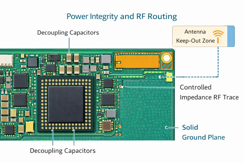
Power Integrity RF Routing HDI PCB: Continuous ground reference protects RF performance and reduces EMI
Before Gerber release, the design should confirm:
In practice, early collaboration between design teams and experienced HDI manufacturers such as NextPCB helps validate stackup feasibility, via strategy, and electrical assumptions before fabrication begins. This alignment significantly improves production predictability and reduces redesign cycles.
At this stage, the PCB is electrically complete — but not yet production-ready. Many HDI boards that pass ERC and DRC still fail during fabrication because design limits were pushed beyond practical manufacturing capability. This step converts the layout into something that can be built reliably and repeatedly.
>> High-Density-Interconnect PCB Manufacturing Capabilities at NextPCB
HDI PCB Microvia Features DFM: Manufacturing limits define reliable HDI microvia implementation
HDI features are reviewed against proven process capabilities:
This prevents common HDI risks such as solder wicking, voiding, alignment sensitivity, and yield instability.
The selected 1+4+1 stackup is checked against actual fabrication flow:
Before generating final fabrication data, a DFM review validates:
After stackup selection, placement optimization, controlled fanout, and DFM validation, the compact IoT controller moved from concept to build-ready without redesign cycles. That alone is the biggest success indicator in dense HDI projects.
Using a controlled HDI approach (not aggressive, not over-engineered), the final board achieved:
The board did not require stackup changes, emergency layer additions, or last-minute fanout modifications — which are common failure points in compact designs.
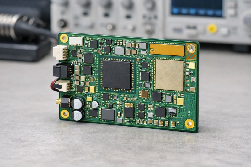
Compact HDI IoT Controller Final Board: Production-ready compact IoT controller designed using disciplined HDI workflow
This approach makes sense when:
It is not necessary when routing completes cleanly on a 4–6 layer board. HDI should solve a problem — not create one.
HDI itself does not increase complexity. Unplanned HDI increases complexity. When applied early, selectively, and aligned with manufacturing capability, HDI becomes a routing stabilizer — not a cost risk.
From a production standpoint, success depends on aligning design intent with fabrication reality. Collaboration with an experienced HDI manufacturer such as NextPCB helps ensure that microvias, stackups, and fanout strategies remain buildable — enabling a smooth transition from prototype to volume manufacturing.
As IoT devices trend toward miniaturization and high performance, High-Density Interconnect (HDI) technology has shifted from "optional" to "essential." Here are the core questions and solutions engineers face when designing space-constrained IoT hardware.
Q1: Which stackup structure is recommended for a first-time HDI IoT project?
A: For most compact IoT controllers (like wearables or sensor nodes), a 1+N+1 structure is the recommended starting point.
Definition: This involves adding one layer of laser-drilled blind vias on the top and bottom of a traditional multilayer core (N).
Why it works: It is the most cost-effective entry into HDI. It handles 0.5mm pitch BGA fanouts easily without the exponential cost increase of multiple lamination cycles. Move to 2+N+2 only if your BGA pitch drops below 0.4mm.
Q2: What are the Aspect Ratio limits for Microvias in HDI?
A: The aspect ratio is the single most important factor for manufacturing yield. To ensure reliable copper plating, you must follow this rule of thumb:
The Golden Ratio: Maintain an Aspect Ratio = (Drill Depth / Drill Diameter) ≤ 0.75:1.
Practical Example: If your dielectric thickness is 3 mil, your laser drill diameter should be at least 4 mil. Exceeding this ratio leads to uneven plating and potential open circuits.
Q3: Is Via-in-Pad mandatory for compact IoT designs?
A: In space-constrained layouts, traditional "dog-bone" fanouts consume too much real estate. Via-in-Pad is often the only viable solution.
The Catch: You must use POFV (Plated Over Filled Via) technology.
Pro Tip: Always specify non-conductive resin filling and capping. If you use open vias in pads, solder paste will wick into the hole during reflow, causing "tombstoning" or weak solder joints.
Q4: How does HDI improve Signal Integrity (SI) for IoT RF circuits?
A: HDI isn't just about saving space; it’s a performance booster for 2.4GHz (Wi-Fi/Bluetooth) and Sub-G signals:
Lower Parasitics: Microvias have significantly lower parasitic capacitance and inductance compared to standard through-holes.
Eliminating Stubs: Blind and buried vias eliminate through-hole "stubs"—the unused portion of a via that acts as a resonant antenna, causing signal reflections and EMI issues.
Q5: How can I keep HDI manufacturing costs under control?
A: HDI is perceived as expensive, but you can optimize the price by following these "Reddit-proven" strategies:
This project shows that HDI PCB design for compact IoT controllers is not about complexity—it is about control. By planning HDI from the start, selecting a practical 1+N+1 stackup, optimizing placement and validating fanout, power and RF early, the design moved cleanly from concept to production-ready hardware.
Instead of increasing risk, HDI reduced routing congestion and improved stability because it was applied selectively and aligned with manufacturing limits. With early DFM review and realistic via choices, the controller scaled smoothly from prototype to volume. For teams building space-constrained IoT products, this structured approach provides a repeatable path to reliable, manufacturable designs—especially when supported by an experienced HDI manufacturing partner like NextPCB.
>>> Recommend reading:
Still, need help? Contact Us: support@nextpcb.com
Need a PCB or PCBA quote? Quote now


 Surface

