

 NextPCB Capabilities
 PCB Assembly
 Layer Buildup
 SMD-Stencils
 PCB Design-Aid & Layout
 Mechanics
 Surface
 Quality
 Drills & Throughplating
 Factory & Certificate


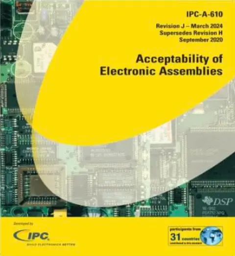
What is the IPC-A-610 Standard?
IPC-A-610, developed by IPC (Association Connecting Electronics Industries), is the globally accepted benchmark for defining visual acceptability of electronic assemblies – critically, Printed Circuit Board (PCB) Assemblies (PCBA). First released in 1983 and consistently updated (with IPC-A-610J being the current 2024 revision), it provides a common language for quality assessment across the PCB manufacturing and assembly (PCBA) industries.
Revision J, released in March 2024, made three notable updates over the previous H revision (2020): expanded and clarified conformal coating inspection criteria (including voiding and bubble assessment), a substantially larger set of visual reference images to improve inspection consistency across facilities, and refined guidance for newer surface-mount component types. Earlier revisions include IPC-A-610H (2020, which removed the "target condition" category and added guidance for bottom-terminated components such as QFNs and LGAs) and IPC-A-610G (2017). IPC skips the letter "I" in its revision naming to avoid confusion with the number 1.
Understanding and applying IPC-A-610 is fundamental to achieving consistently high-quality and reliable PCB assemblies. The standard establishes specific, measurable criteria to evaluate the suitability and longevity of PCBA. It covers critical areas including:
- Component Placement (orientation, alignment, spacing on PCB)
- Soldering Quality (SMT, through-hole, mixed)
- Cleanliness (post-assembly residue control affecting PCB reliability)
- Marking/Labeling (for PCB and component traceability)
By employing systematic inspection based on IPC-A-610, PCB manufacturers and PCBA service providers (like NextPCB) can objectively ensure their assemblies meet stringent functional and aesthetic requirements vital for end-product success. This standard is indispensable for:
- Electronics Manufacturers & Assembly Houses: Setting internal PCBA quality control processes.
- Inspection Organizations: Providing unbiased assessments.
- Customers & Suppliers: Establishing clear, mutually understood quality requirements and acceptance criteria for PCBA.
- Regulatory Agencies: IPC-A-610 is consistently updated to address the evolving requirements of key industries such as aerospace, automotive PCB assembly, and medical device PCBA manufacturing.
IPC-A-610 (J) is the globally recognized benchmark for electronic assembly quality, providing a unified visual language for the industry.
>> Recommend reading: PCBA Rework & Repair
Key IPC-A-610 Acceptance Criteria for PCB Assemblies (PCBA)
Understanding Requirements for SMT, Through-Hole & Mixed Technology PCBA
However, by incorporating IPC-A-610 standards, you can ensure the quality of your electronic assemblies — from through-hole to mixed technology. This set of criteria is based on inspection and evaluation parameters. They are component placement, soldering accuracy, cleaning levels and marking regulations. Therefore, here are some examples of what they include:
Through-Hole Component Requirements on PCB Assembly
For through-hole components, the acceptance criteria include the following:

Standard through-hole mounting on NextPCB's own assembly line: IPC-A-610 specifies strict requirements for lead protrusion, solder wetting, and component alignment.
- Proper component orientation, spacing, and alignment on the PCB substrate
- Secure mounting of components to the PCB to withstand operation strains
- Sufficient lead length for robust PCB soldering
- Avoidance of solder bridging which can cause PCB failures
- No damage to component leads or PCB lands
- No excessive solder, solder bridging, or cold solder joints
- No visible cracks or fractures in the solder joints
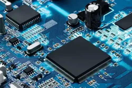
Surface Mount (SMT) Component Requirements for Reliable PCB Assembly
For surface-mount components, the acceptance criteria include the following:

Photographed on NextPCB's SMT line: inspection focuses on critical parameters such as fillet height, toe/heel overhang, and solder paste coverage.
- Proper component orientation, spacing, and alignment
- No damage to the component, PCB, or solder joint during assembly
- Proper solder joint formation, including wetting and fillet formation
- No visible voids, excessive solder, or solder bridging
- No lifted, tilted, or misaligned components
Mixed-Technology PCB Assembly: Combining SMT & Through-Hole Standards
For mixed-technology assemblies, the acceptance criteria combine the requirements for through-hole and surface-mount components. Furthermore, this includes ensuring that the through-hole components are properly mounted and soldered. Similarly, the surface-mount components have proper solder joint formation and component orientation.
A mixed-technology board from an actual NextPCB assembly run: production requires a balanced application of both THT and SMT standards to ensure overall system reliability.
IPC-A-610 is an invaluable asset for upholding quality in electronic assemblies, providing specific acceptance criteria to guarantee that products meet the necessary standards. Whether it's cleaning and coating necessities, marking or labeling specifications, or testing requirements - all components are thoroughly evaluated to make sure they can fulfill their desired purpose.
Component Placement Requirements
Securing components in the right position is essential for a successful electronic assembly, and IPC-A-610 furnishes guidelines on where these parts should be placed. This holds true regardless of whether it's through-hole, surface mount or mixed technology assemblies - covering all your basis. Furthermore here are some key factors to consider when you place them:
- Component orientation: The orientation of components should be correct, with all components properly aligned in the direction specified in the assembly documentation. The orientation of polarized components, such as electrolytic capacitors and diodes, should also be verified.
- Spacing and alignment: Components should be placed at the correct spacing and alignment to ensure proper clearance, avoid mechanical interference, and provide sufficient room for assembly and testing.
- Mounting: Components should be securely mounted to the PCB, with all leads or pads properly inserted or seated. The component leads or pads should not be damaged during insertion, and the component should be held in place until soldered.
- Through-hole components: For through-hole components, the leads should be trimmed and bent at the correct length and angle to ensure proper solder joint formation. The leads should also be flush with the PCB surface to avoid mechanical interference with other components.
- Surface-mount components: For surface-mount components, the placement of the components should be accurate and consistent, with proper alignment and spacing. The orientation of the components should also be verified to ensure that they are correctly placed before soldering.
Furthermore, the criteria for component placement are designed to ensure that electronic assemblies are properly assembled and meet the quality standards required for their intended use. Failure to meet these criteria can result in assembly defects and can affect the functionality and reliability of the finished product.
Soldering Requirements According to IPC-A-610

Key indicators of a reliable solder joint include a smooth, concave fillet and a clear transition between the pad and component lead.
Soldering is an essential part of electronic assembly, and IPC-A-610 supplies parameters when it comes to soldering for various types of assemblies: from through-hole, surface mount, and combined technology. The criteria for this type of process include the following aspects:

Taken from a real inspection at NextPCB: post-solder residue checks define acceptable levels of flux residue to prevent electrochemical migration.
Solder joint formation
The formation of the solder joint should be consistent and uniform, with no voids, excessive solder, or solder bridging. The solder should also wet the pad or lead surface completely to ensure a strong and reliable joint.
Solder joint fillet
The fillet of the solder joint should be smooth and concave, with a visible transition between the pad or lead surface and the solder. The fillet should also be continuous and uniform around the entire perimeter of the joint.
Solder joint shape
The shape of the solder joint should be appropriate for the type of component and the intended use of the assembly. Moreover, as an example, the solder joint for through-hole components should be barrel-shaped, while the solder joint for surface-mount components should be a flat or slightly concave shape.
Solder cleanliness
The solder joint and surrounding area should be free of flux residues, debris, or other contaminants that can affect the reliability of the joint.
Solder joint strength
The solder joint should be strong and mechanically sound, with no visible cracks or fractures. The joint should also be able to withstand the stresses and strains of assembly, testing, and use.
The criteria for soldering are designed to ensure that electronic assemblies are properly assembled and meet the quality standards required for their intended use.
Cleaning and Coating Requirements According to IPC-A-610
Maintaining and coating your electronic components is essential for guaranteeing the product's dependability and functionality. IPC-A-610 provides criteria for cleaning and protecting through-hole, surface mount, as well as mixed technology assemblies. This criterion includes:

NextPCB technicians performing localized cleaning with ESD-safe tools—vital for removing contaminants and ensuring proper adhesion for conformal coatings.
Cleaning requirements for PCB Assembly (PCBA):
The assembly should be cleaned after soldering to remove flux residues, debris, or other contaminants that can affect the reliability of the assembly. The cleaning method should be appropriate for the type of assembly and the cleaning agent used should not damage the assembly or components.
Coating requirements for PCBA:
The assembly may be coated with a conformal coating to provide additional protection against environmental factors such as moisture, dust, and chemical exposure. The coating should be applied uniformly and consistently, with no voids, bubbles, or other defects that can affect the reliability of the assembly.
Coating thickness for PCBA:
The coating thickness should be appropriate for the intended use of the assembly. Therefore, should not affect the functionality or performance of the assembly. The thickness of the coating can be measured using appropriate tools and should be within the acceptable range.
Coating material for PCBA:
The coating material should be appropriate for the type of assembly and the intended use of the assembly. The coating material should also be compatible with the materials used in the assembly. Moreover, should not affect the functionality or reliability of the assembly.
Marking and Labeling Requirements
Accurate and decipherable labeling is critical to electronic assembly, allowing recognition and tracking of the entire unit as well as its components. IPC-A-610 outlines criteria for marking and labeling different types of electronic assemblies including through-hole, surface mount, or mixed technology. Clearl includes but is not limited to:
- Component marking: Components should be marked with appropriate identification codes or symbols to enable identification and traceability. The marking should be legible, permanent, and located in a visible area of the component.
- PCB marking: The PCB should be marked with appropriate identification codes or symbols to enable identification and traceability. The marking should be legible, permanent, and located in a visible area of the PCB.
- Assembly marking: The assembly should be marked with appropriate identification codes or symbols to enable identification and traceability. The marking should be legible, permanent, and located in a visible area of the assembly.
- Labeling: The assembly may require labeling to provide additional information or instructions to the end user. The labeling should be legible, permanent, and located in a visible area of the assembly.
- Location and orientation marking: The location and orientation of components should be marked on the PCB. This is to enable accurate placement and ensure proper functionality and reliability of the assembly
Training and Certification Requirements
If you're involved in the production of electronic assembly, IPC-A-610 offers a training and certification program tailored to guarantee that any individual has the required understanding and capabilities to complete their tasks productively and with excellence. The key components of this education & qualification procedure consist of:
- Training program: The training program should cover the relevant topics and criteria specified in IPC-A-610. And should be delivered by certified trainers or training centers. The program may include classroom instruction, practical exercises, and examinations.
- Certification program: The certification program should include examinations to assess the knowledge and skills of the individuals specified in IPC-A-610. The certification program may consist of different levels of certification, depending on the individual's job function and responsibilities.
- Recertification: Certified individuals may be required to undergo recertification periodically. This is to ensure that their knowledge and skills are up-to-date and to the standards required by the industry.
- Training records: Training records should be maintained for each individual who undergoes IPC-A-610 training and certification. The records should include the individual's name, date of training and certification, certification level, and any other relevant information.
Conclusion
IPC-A-610 is far more than a static document; it's the cornerstone of quality, performance, and reliability assurance in PCB assembly (PCBA). By meticulously defining criteria for component placement, soldering excellence, cleanliness, and traceability (marking/labeling), this standard equips PCB manufacturers and PCBA suppliers with the objective metrics needed to guarantee products meet the rigorous demands of their intended applications – from consumer electronics to IPC Class 3-rated high-reliability PCB assemblies for aerospace or medical devices.
Adherence to IPC-A-610, coupled with rigorous training and certification of personnel (as outlined in the standard), is not merely about compliance; it's about delivering confidence. It ensures PCB assemblies (PCBA) not only meet customer expectations but consistently deliver the operational longevity and robustness demanded by today's complex electronic systems.
At NextPCB, IPC-A-610 compliance isn't a checkbox; it's deeply embedded throughout our advanced PCB manufacturing and PCBA processes. Our expertise in interpreting and applying this standard – particularly the stringent demands of Class 2 and Class 3 PCB assembly – ensures we deliver uncompromising quality and reliability to our partners across diverse industries. Trust NextPCB to build your success on the foundation of IPC-A-610 standards.
Ready to partner with an IPC-A-610 expert for your next high-quality PCB Assembly project?
Get Your Instant PCBA Quote Now
Explore NextPCB's Advanced PCBA Capabilities
Mastering IPC-A-610: Frequently Asked Questions on PCB Assembly Standards
Navigating the complexities of PCB assembly (PCBA) quality can be daunting. Based on trending discussions among engineers on Reddit and industry forums, we’ve compiled the most critical questions regarding the IPC-A-610 standard—the global benchmark for electronic assembly acceptability.
Frequently Asked Questions
Q1: What is the main difference between IPC Class 2 and Class 3?
The primary difference lies in the reliability and environment of the final product:
- Class 2 (Dedicated Service Electronic Products): Covers equipment where continued performance and extended life are required, but uninterrupted service is not critical (e.g., computers, household appliances).
- Class 3 (High-Performance/Harsh Environment Electronic Products): For mission-critical applications where downtime is not an option, such as medical life support, aerospace, and military systems.
- Key Technical Gap: Class 3 requires a higher degree of inspection and stricter tolerances, such as a 75% vertical solder fill in through-holes, compared to 50% for Class 2.
For the full breakdown of every criterion that differs between Class 2 and Class 3—including annular ring, overhang, and coating requirements—see our dedicated guide: IPC Class 2 vs 3: The Differences in PCB IPC Standards.
Q2: How much "Solder Voiding" is acceptable in BGA and QFN packages?
Solder voids (air bubbles) are a common concern in X-ray inspections. According to IPC-A-610:
- Generally, a void is considered acceptable if it occupies less than 25% of the total solder ball area in a BGA joint.
- However, for thermal pads on QFNs, the requirements can vary based on the design's heat dissipation needs. While 25% is the standard rule of thumb, high-power applications may require even stricter limits to prevent overheating.
Q3: Is component misalignment (overhang) always a defect?
Not necessarily. IPC-A-610 provides specific "Acceptable" vs. "Defect" criteria for component placement:
- Side Overhang: For most classes, a component can hang off the side of the land (pad) by up to 25% or 50% of its width (depending on the class and component type) without being classified as a defect.
- The Golden Rule: As long as the minimum electrical clearance is maintained and the solder joint remains robust, a slight misalignment is often "Acceptable."
Q4: Do I need to clean "No-Clean" flux residues to meet IPC standards?
This is a frequent debate in the engineering community. Under IPC-A-610:
- No-Clean Flux residues are acceptable as long as they are non-corrosive, non-conductive, and do not interfere with visual inspection or testing.
- The Risk: In high-humidity environments, even "no-clean" residues can lead to Electrochemical Migration (ECM) or dendritic growth. If your board operates in harsh conditions, we recommend professional cleaning regardless of the flux type used.
Q5: Why does IPC-A-610 prioritize "Visual Acceptance" over process control?
IPC-A-610 is specifically a visual acceptance standard. It defines what the final product should look like. It does not dictate how to build it (that would be IPC-J-STD-001). For customers, this means IPC-A-610 is your quality checklist to ensure the boards you receive from a manufacturer like NextPCB meet international reliability benchmarks.
Summary Table: IPC-A-610 Quick Reference
| Feature | Class 1 (General) | Class 2 (Dedicated) | Class 3 (High-Rel) |
|---|---|---|---|
| Application | Consumer Electronics | Industrial/Business | Medical/Aerospace |
| Through-Hole Fill | Not specified | 50% minimum | 75% minimum |
| Component Overhang | Most lenient | Moderate | Strictest limits |
| Inspection Rigor | Visual Sample | Thorough | 100% Inspection/X-Ray |
Beyond Assembly Inspection: While IPC-A-610 defines electronic assembly acceptability, it works hand-in-hand with J-STD-001 for soldering and IPC-A-600 for bare boards. Access the complete, interconnected ecosystem at our IPC Electronic Standards Hub.
More IPC Standard Articles:
- > IPC Class 2 vs 3: The Differences in PCB IPC Standards
- > Master IPC-A-600: The Definitive Guide to PCB Inspection & Acceptability
- > IPC 6012 Guidelines: Classifying, Designing, and Fabricating PCBs
- > IPC-J-STD-001: Top Guide to the Latest IPC Soldering Standards (J Revision)
- > PCBA Rework and Repair Technical Guide: Mastering IPC-7711/7721

