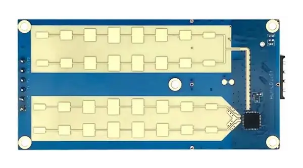
Thick copper PCB is widely used in power electronic equipment and power supply systems. The growth trend of the PCB industry is that the finished copper weight exceeds 4oz (140μm), while the copper weight of the standard PCB is usually 1oz (35μm) or 2oz (0μm).
The extra copper of PCB allows the printed circuit board to conduct more current and achieve excellent heat distribution, which can realize complicated functions in a limited space. Other advantages include improving the mechanical strength of the connector position, the ability to make the smaller sizes of products by combining multiple weights on the same circuit layer, and the ability to use exotic materials with maximum capacity and minimize the risk of circuit failure.
Advantages of thick copper PCB:
1) Greatly increase the current capacity
2) Higher resistance to thermal strain
3) Better heat dissipation
4) Increase the mechanical strength of the connector and PTH hole
5) Reduce product size
Application of thick copper PCB:
With the increase of high-power products, the demand for thick copper PCBs has also greatly increased. Nowadays, PCB manufacturers pay more attention to the use of copper plates to solve the thermal efficiency problem of high-power electronic equipment.
Thick copper PCBs are mostly high-current substrates. The high-current PCBs are mainly used for power modules and automotive electronic parts. Now, copper PCB has replaced the transmission form, which will not only increase productivity and reduce the time cost of wiring but also improve the reliability of the final product. At the same time, the high current board can increase the design freedom of wiring, thereby achieving the miniaturization of the entire product.
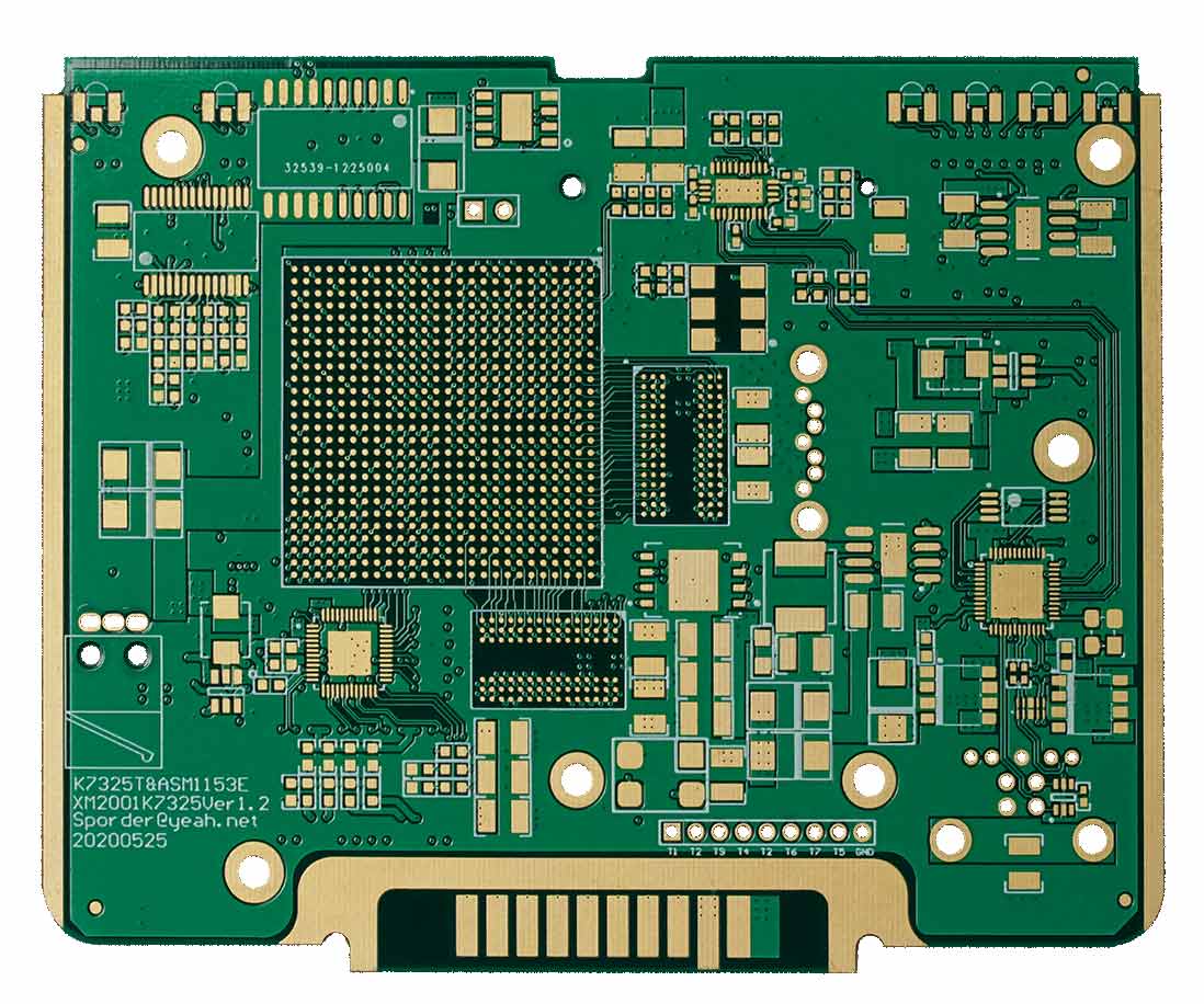
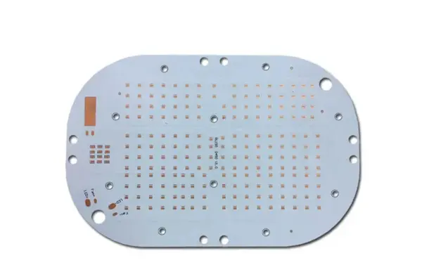
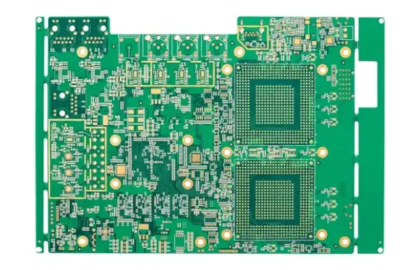
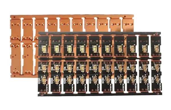
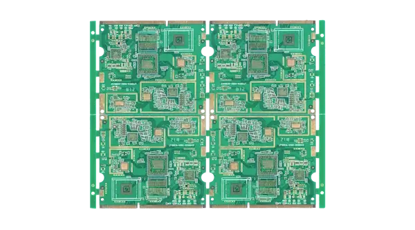
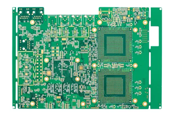
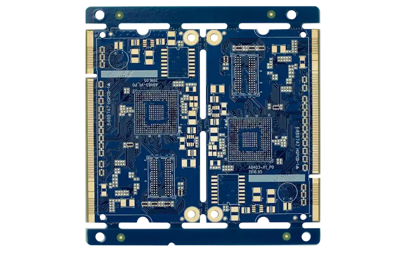
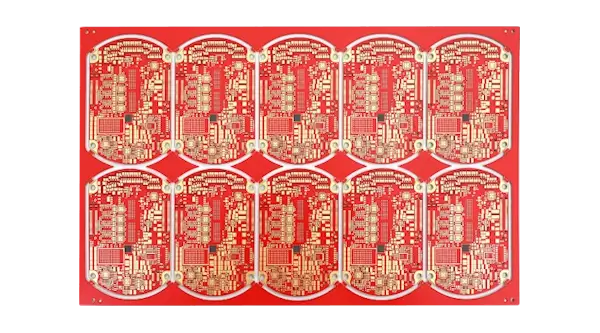
NextPCB is a skilled PCB manufacturer that can develop and produce high-quality copper PCB. The maximum copper weight of thick copper PCB on NextPCB is 2oz. Check the functions in the table below:
Thick copper PCB introduction
|
Items
|
Manufacturing Capabilities
|
|
Material
|
FR-4 Standard Tg 140°C, FR4-High Tg 170°C
|
|
Min. Track/Spacing
|
For External layers:
4oz Cu 9mil/9mil,5oz Cu 11mil/11mil
6oz Cu 13mil/13mil,12oz Cu 20mil/32mil
For Internal layers:
4oz Cu 8mil/12mil,5oz Cu 10mil/14mil
6oz Cu 12mil/16mil,12oz Cu 20mil/32mil
|
|
Min. Hole Size
|
10mil
|
|
Max Outer Layer Copper Weight (Finished)
|
2oz
|
|
Max Inner Layer Copper Weight
|
2oz
|
|
Board Thickness
|
0.6-6mm
|
|
Surface Finishing
|
Immersion gold, OSP, Hard Gold, Immersion Silver, ENEPIG
|
|
Solder Mask
|
Green, Red, Yellow, Blue, White, Black, Purple, Matte Black, Matte green
|
|
Silkscreen
|
White, Black
|
|
Via Process
|
Tenting Vias, Plugged Vias, Vias not covered
|
|
Testing
|
Fly Probe Testing (Free) and A.O.I. testing
|
NextPCB has 15 years of experience in PCB manufacturing and PCB assembly of copper PCB, requesting skilled engineers to check each circuit file and solve all problems before production, which helps to ensure that the finished circuit board meets your performance expectations. Our quality control department will also guarantee the quality of printed circuit boards.
>> Advanced PCB Capabilities - NextPCB

 NextPCB Capabilities
 PCB Assembly
 Layer Buildup
 SMD-Stencils
 PCB Design-Aid & Layout
 Mechanics
 Surface
 Quality
 Drills & Throughplating
 Factory & Certificate