
 NextPCB Capabilities
Printed Circuit Boards
NextPCB Capabilities
Printed Circuit Boards
 PCB Assembly
 Layer Buildup
 SMD-Stencils
 PCB Design-Aid & Layout
 Mechanics
 Quality
 Drills & Throughplating
 Factory & Certificate
 PCB Assembly Factory Show
Certificate
PCB Assembly Factory Show
Certificate

Support Team
Feedback:
support@nextpcb.com
Fast, affordable online PCB prototyping — 1–32 layers, HDI, rigid-flex, no MOQ. Trusted by 100,000+ engineers worldwide. ISO 9001 & IATF 16949 certified.
15+ years as a prototype PCB manufacturer. ISO 9001, IATF 16949, ISO 14001 certified.
Full capabilities ›
1–2 layer prototypes dispatched in 24 hours. 4-layer in 48 hours. The fastest path from Gerber file to physical board.
2-layer prototypes from $5 with no hidden fees. Instant online pricing — no waiting for a manual quote.
Single-sided boards through 32-layer HDI. Rigid, flex, rigid-flex, and high-frequency Rogers materials all supported.
Up to 10 prototype units tested for free before shipment — validating electrical performance under real conditions.
Automatic DFM analysis on every upload. Catch manufacturability issues before production starts, not after.
Order as few as 1 board. No setup fees or minimum quantities — ideal for first-spin prototypes and design validation.
600,000+ genuine in-stock parts via HQ Online. Combine PCB + assembly into a single turnkey order.
Worldwide shipping via DHL, FedEx, and UPS. Tracked delivery to 170+ countries with duty-inclusive options available.
Select the layer configuration that fits your design complexity and budget. Not sure which to choose? Upload your Gerber and we’ll advise.
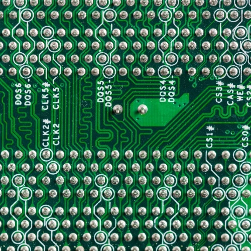
The fastest and most affordable prototype format. Double-sided copper routing supports the vast majority of standard circuit designs—from microcontroller boards and sensor modules to power supplies and LED drivers. 24-hour quick-turn as standard.
Materials: FR-4 (TG130 / TG150 / TG170), FR-1 · Surface finish: HASL, ENIG, OSP, Immersion Silver · Copper: up to 10 oz
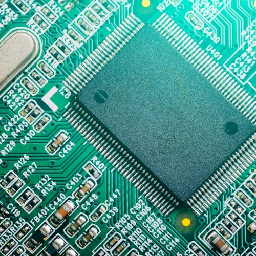
Two internal copper layers dedicated to power and ground planes — enabling tighter signal integrity, reduced EMI, and higher component density than a 2-layer design. The right choice for FPGAs, high-speed digital, and wireless RF applications. Impedance control to ±5% available.
Surface finish: ENIG, HASL, Immersion Silver, OSP, ENEPIG · Substrate: FR-4, High-TG, Rogers · Copper: up to 10 oz
Engineered for demanding architectural tiers, complex signal routing, and ultra-high frequency requirements. Fully compliant with rigid IPC Class 2/3 manufacturing parameters, offering standard DFM, DFA, and signal integrity validation.
No lengthy RFQ process. Upload, configure, pay, and track — all online.
Accepts Gerber RS-274x, Gerber X2, and ODB++. Exported from Altium, KiCad, Eagle, OrCAD, and more.
Configure layers, size, finish, quantity, and turnaround. Price updates in real time — no waiting for a salesperson.
Our HQDFM engine automatically checks your files for manufacturability issues before production starts.
Quick-turn production starts same day. Boards are tested, packed, and shipped via DHL / FedEx / UPS with full tracking.
Transparent pricing with no hidden fees. Every quote is generated instantly online — no manual negotiation required.
| PCB Type | Starting Price | Quick-Turn Lead Time | Key Specs |
|---|---|---|---|
| 1–2 Layer | $5 | 24 hours | Up to 1500 × 600 mm; Min 10 × 10 mm; HASL / ENIG; No MOQ |
| 4-Layer | $30 | 48 hours | Impedance control ±5%; blind/buried vias |
| 6-Layer | $60 | 3–5 days | Rigid-flex options; Rogers materials available |
| 8–32 Layer / HDI | Custom | 5–10 days | HDI microvias; Rogers / Arlon; up to 60 GHz |
Larger area = more material and machine time
More layers = more lamination cycles and cost
HASL is cheapest; ENIG adds a small premium
24h quick-turn carries a small speed premium
5–10 pcs vs 1 pc drops unit price significantly
Rogers / high-TG carry a premium over standard FR-4
Instant pricing — no account required to get a quote
Full manufacturing capabilities for standard and advanced PCB prototypes. See our standard and advanced capability pages for the complete parameter list.
| Parameter | Standard (1–2 Layer) | Advanced (4–20 Layer) |
|---|---|---|
| Layer Count | 1–2 layers | 4–20 layers |
| Min. Trace Width / Space | 3.5 mil (0.089 mm) | 3 mil (0.076 mm) |
| Min. Hole Diameter | 0.15 mm (6 mil) |
0.15 mm (6 mil) Mechanical 0.075 mm (3 mil) Laser Microvia |
| Surface Finish | HASL (leaded & lead-free), OSP | ENIG, ENEPIG, Hard Gold, Immersion Silver, Immersion Tin, OSP |
| Board Dimensions | 10×10 mm → 1500*600mm |
4-Layer: up to 1500*600mm 6–20 Layer: up to 500×400 mm |
| Material Selection | Standard Kingboard (KB) or Shengyi (SY) FR-4 laminates, FR-1 | A-Grade High-TG170, Rogers (RO3000/RO4000), Megtron 6/7, Isola, ITEQ composites |
| Impedance Control | ±10% | ±10% (±5% available upon structural request via coupon testing) |
| Copper Thickness | Up to 10 oz inner & outer layers | |
| Solder Mask Colors | Green, Blue, Red, Yellow, White, Black, Matte Black, Matte Green | |
| Special Processes & Customization | Not available for standard quick-turn | Any-layer HDI infrastructure, blind & buried vias, backdrilling, embedded copper coins, conductive/non-conductive epoxy via filling, hybrid/asymmetric custom stackups, counterbore/countersunk holes, castellated holes, edge plating, carbon ink |
| Accepted File Formats | Gerber RS-274x, Gerber X2, ODB++ — exported from Altium, KiCad, Eagle, OrCAD, etc. | |
| Other Board Types | Metal Core (MCPCB), Flexible PCB, Rigid-Flex, Ceramic, Aluminum substrates | |
Comprehensive QC options tailored to your design complexity before shipment. ISO 9001, IATF 16949, UL, RoHS, and REACH certified. View certificates ›
Automated optical inspection for surface defects on every layer
Verifies multilayer registration and hidden solder joint integrity
Coupon-based measurement confirms trace impedance to ±5%
Confirms connectivity; detects shorts and opens
Real-condition performance verification for up to 10 prototype units at no charge
Camera-guided drilling with automated registration correction
Adhesion and dimensional accuracy checks for long-term durability
ISO 9001 · IATF 16949 · ISO 14001 · UL · RoHS · REACH
From individual makers to Fortune 500 engineering teams — 100,000+ customers in 170+ countries.
Design validation before mass production
Investor demos and funding-round prototypes
Rapid iteration on new product development
Custom boards, Arduino shields, open-source hardware
Student projects and academic research boards
NextPCB also offers PCBA prototype services — components sourced, placed, and soldered. Bare PCB prototype and PCBA prototype are different services with different lead times and pricing.
Common questions about ordering PCB prototypes online from NextPCB.
A 2-layer prototype at NextPCB starts from $5 (up to 100×100 mm). A 4-layer prototype starts from $30.
Price depends on board size, layer count, surface finish, quantity, and turnaround. Use our instant quote tool for an exact figure.
NextPCB offers 24-hour quick-turn for 1–2 layer prototypes and 48-hour for 4-layer boards. Shipping time is additional depending on your location and carrier.
Choose 2-layer for simple circuits, hobbyist projects, and cost-sensitive prototypes. It’s the cheapest and fastest option.
Choose 4-layer when you need dedicated power/ground planes, tighter signal integrity, lower EMI, or higher component density — typical for FPGA, high-speed digital, or wireless RF designs.
Yes. NextPCB has no MOQ for PCB prototypes. Order as few as 1 piece. The entire process — quote, payment, and order tracking — is online with no account required to get a quote.
Upload Gerber RS-274x, Gerber X2, or ODB++ files. Supported design tools include Altium Designer, KiCad, Eagle, and OrCAD. Our system auto-parses layers and runs a free DFM check on upload.
Yes — free functional testing for up to 10 prototype units, verifying real-condition electrical performance at no extra cost. Full details ›
A PCB prototype is a bare printed circuit board — no components. This is the service described on this page.
A PCBA prototype has components sourced, placed, and soldered onto the board, ready for functional testing. NextPCB offers both. Explore PCBA services ›
2-layer boards from $5 · 24-hour quick-turn · No MOQ · Free DFM check · 170+ countries served
Instant online pricing — no account required to get a quote
Questions? support@nextpcb.com · +86-755-8364-3663 · Help Center


 Surface

