
 NextPCB Capabilities
Printed Circuit Boards
NextPCB Capabilities
Printed Circuit Boards
 PCB Assembly
 Layer Buildup
 SMD-Stencils
 PCB Design-Aid & Layout
 Mechanics
 Quality
 Drills & Throughplating
 Factory & Certificate
 PCB Assembly Factory Show
Certificate
PCB Assembly Factory Show
Certificate
Support Team
Feedback:
support@nextpcb.com


The author of this article is Titov Oleg Andreevich, the owner of Zen channel《Разумный мир》. This article is the English version of 《DFM, DFMA, DFA. Часть 2. Приложение от NextPCB для ПК》
In the previous article, we got acquainted, albeit very briefly, with what DFM is. And we saw how NextPCB Online Gerber Viewer works and what it can offer. Today we'll get to know the more functional DFM Analysis Tool application, which is installed on a PC. Let's see how it differs from the NextPCB Online Gerber Viewer. For this purpose, we will use the same sets of Gerber files as in the previous article
At the same time, we will touch only on part of all the capabilities of the application.
You can download the installer from the following pages:
Аnd it is immediately clear that the program is for Windows only. For most readers, this will not be a problem, but for those who use Linux, it is not the happiest news. But let's not get ahead of ourselves. No other system or hardware requirements are specified. The installation program is downloaded as an archive HQDFM_en.zip, there is a single exe-file, the installer itself. The installation is simple and standard, so there is no point in going into more detail. And the installation goes without errors both in Windows on a real PC, and in Linux under Wine, and in Windows running on VirtualBox virtual machine under Linux.
But then everything is not so easy and simple... I have bad news for Linux users. Under Wine, the program crashes with an error right after launching. It does not depend on the bit size (32 or 64) and the version of the wine. But not all Windows programs work under Wine, so the result is not entirely unexpected. Under VirtualBox, if 3D support is disabled, the program reports a problem with OpenGL at startup, but the error message can be closed. HQDFM even tries to work, but after any action, the window with the PCB image freezes for a couple of minutes. If you enable 3D support, the program starts without errors, but the PCB image window always remains empty.
HQDFM program cannot work under Linux. Neither under wine, nor under VirtualBox, nor under QEMU/KVM. Perhaps I was not persistent enough, but I have to state that to run the program you need a real PC with Windows.
However, things may not be so simple on a real PC either. I found two real PCs. One is quite old, without a separate video card, with 64-bit Windows 7. The second one is quite new, with an NVIDIA graphics card, with Windows 10. Under Windows 7 the program refused to work, giving an error message as well as under Wine. But under Windows 10 everything worked as it should.
To work with the HQDFM program you need a full-fledged PC or laptop, and relatively new, preferably with a screen FullHD or better, running under Windows 10. The work under Windows 8 has not been tested, we simply did not find a PC with this version. That's why all the examples in today's article are prepared using Windows 10. I am sure that for many (most) people this will not be a problem.
After the first launch of HQDFM, we will see a window with a prompt to log in or register.
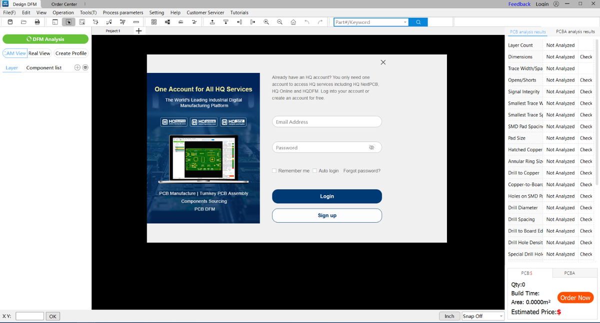
This window can be closed but it will reappear when you try to load Gerber files. Therefore, you need a NextPCB account to work with the program. Registration is simple, we will not consider it.
They do not send spam
I will use my own, specially created, account. Now we can take a closer look at the program window without loaded files. 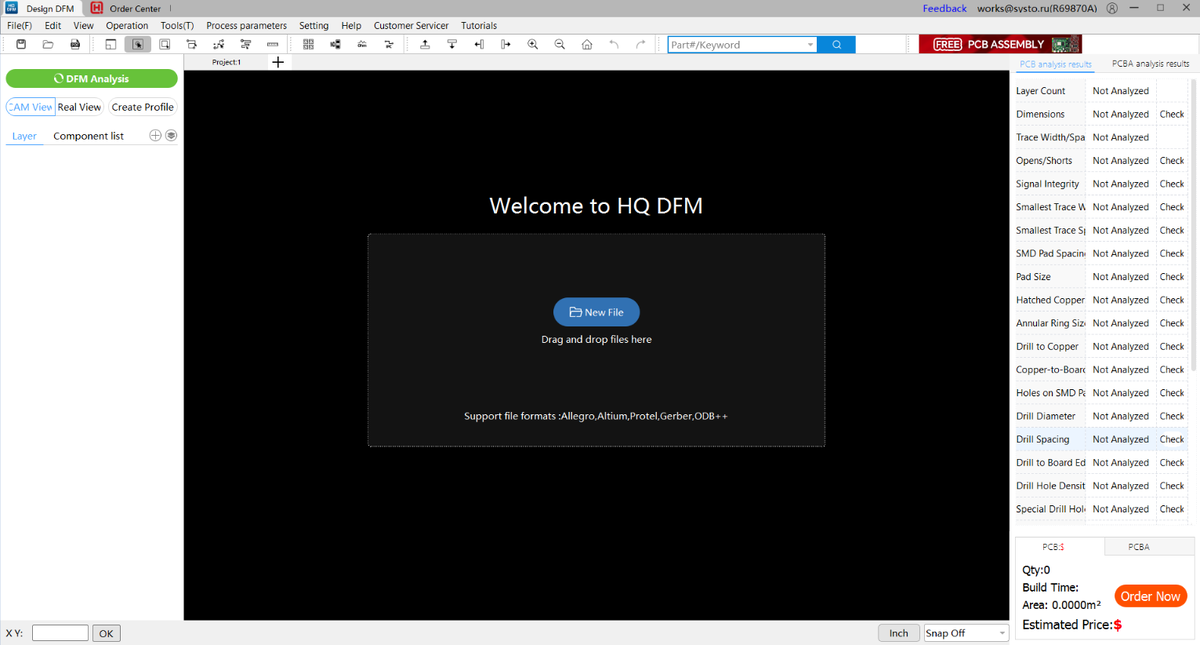
The program window consists of three main parts. In the center is the largest area. This is where our PCB will be displayed. On the left will be displayed the list of layers and components (if we load a BOM file). On the right side is the list of tests performed and the results of the tests. We can already see the difference from NextPCB Online Gerber Viewer - here the list of checks looks much more informative. As we will soon see, it is also more functional.
Let's load the Gerber files of our electronic load power module board, the same set with errors we started with in the previous article. Only now it is the individual files that need to be uploaded, not the archive. The loading is very fast, which is not surprising, and we will see our board 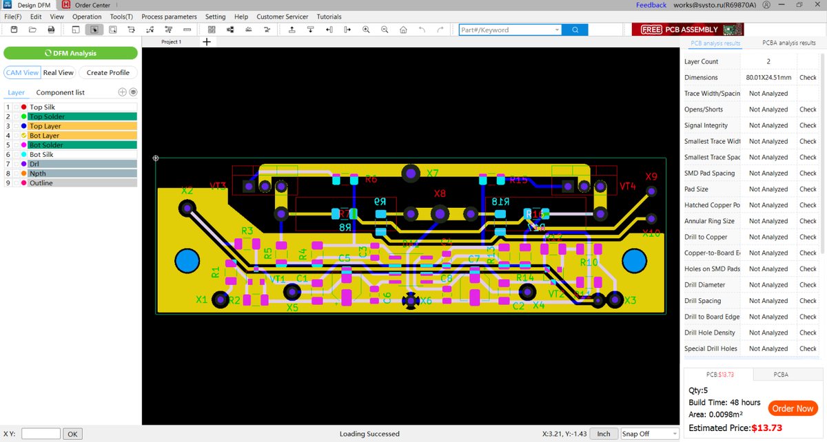
In addition to the board, we now also see a populated list of layers, each layer corresponding to a different file. On the right side of the screen, we can see the number of copper layers and the size of the board. And at the bottom right even the cost of ordering 5 boards (and you can place an order right away, for this they require registration), but we are not interested in that today. But in the upper left corner of the board, you can now see the coordinate origin point we set in KiCad, which was not present in NextPCB Online Gerber Viewer.
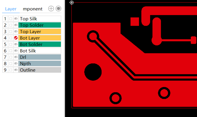
Working with layers is not standard, so let's take a closer look at it. A single click on a layer name in the list toggles its visibility in the PCB display area. Let's turn off the visibility of the B.Cu layer, which is called the "Bot Layer" in HQDFM, by clicking on it once. The effect will be as follows
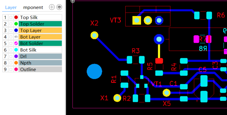
The colored circle in front of the layer name has been replaced by the image of a gray crossed-out eye, indicating that this layer is turned off. The appearance of the board in the area of its display has also changed. Don't pay attention to the strange yellow track and red contact pad, I'll tell you what it means shortly. We can turn on and off any layers, any number of them. Double-clicking on the layer name turns off all layers except the selected one. Unexpectedly, the color of the layer changes to red, and the color of the layer is not restored afterward! The effect of double-clicking on the bottom copper layer is as follows
We can examine the board in enough detail by selecting the layers we need. However, attentive readers noticed that there is no option to enable/disable all layers here. And they were wrong! There are many more options here, it just requires a right-click
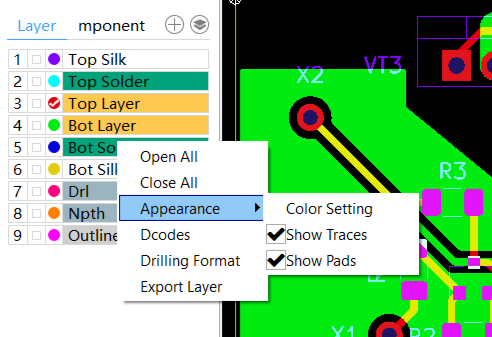
Now we can not only turn the layer on/off but also change its color. And we can see how exactly the elements of our PCB are formed. So the tracks and pads seem to be a single whole, but if we select the Dcodes item in the layer menu (right-click), for example, for the top copper layer, we can see that this is not so
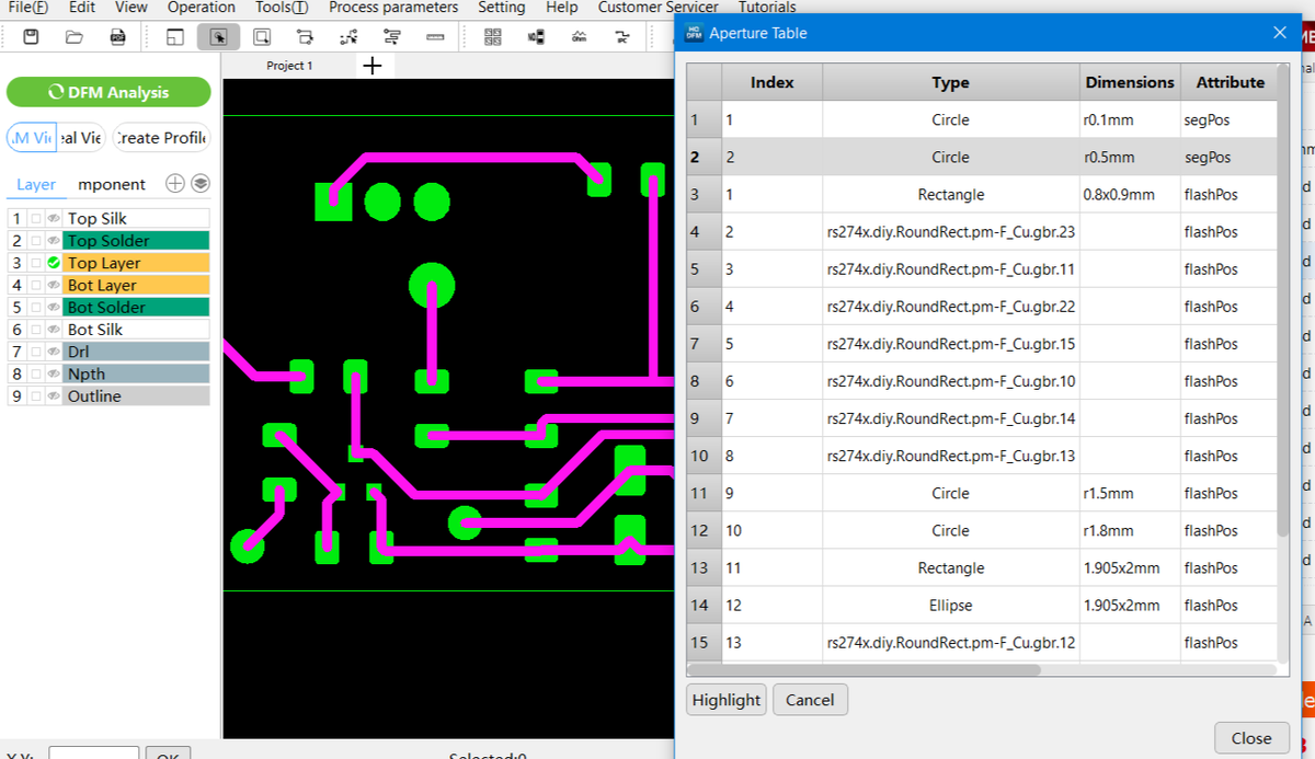
I have selected the desired element in the table, which is used to form the tracks of the top copper layer, and clicked the "Highlight" button. You can clearly see that the tracks are formed separately from the contact pads. And they start and end in the centers of the contact pads. But that's not all. Above the list of layers, you can see two buttons 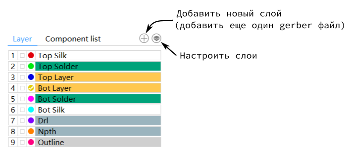
If we forget to add some gerber file (layer) we can easily add it at any time. But more interesting is the ability to customize layers 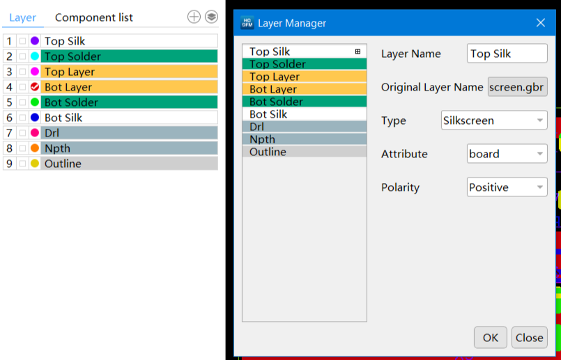
There is no way to change the color of a layer here, we've already seen where that is done. But here you can change the layer name and its type. I chose the "Top Silk" layer, which the program defined as a silkscreen layer, in full accordance with the Gerber file. We can change the layer type, for example, to "Signal", which corresponds to the copper layer, or to "Solder Mask", which corresponds to the mask layer. "Attribute" allows us to specify whether the layer is placed on the board physically (board) or is an auxiliary/service layer (misc). All this only applies to viewing and analyzing the PCB, the Gerber files themselves are not modified.
Layers have been dealt with, now let's move on to the much more interesting image of the PCB itself. Working with this area is also non-standard, so we will consider it in detail, although not all the available options. Otherwise, this article will turn from a large one into a huge one.
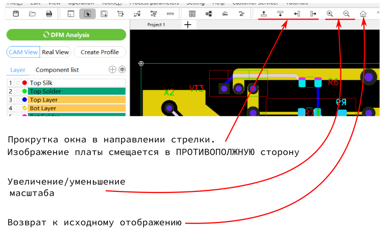
You can change the scale of the board image in the viewing area with the mouse wheel when the "Ctrl" button on the keyboard is pressed. Otherwise, the mouse wheel will only scroll up/down the display area. You can move the image of the board by pressing the right mouse button and moving the mouse. All this can be done through the toolbar, which is located under the program menu bar. But it is faster and more convenient to use the mouse
The left mouse button is used to select various elements of the active layer of the board. The active layer is marked in the layer list by a checkmark on the colored circle before its name. You can see this checkmark in the illustrations above. You can make a layer active by clicking on this colored circle. The visibility of the layer is not switched
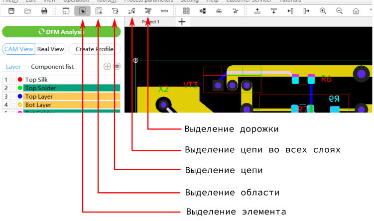
The difference between the selection methods is not quite obvious, so let's take a closer look.
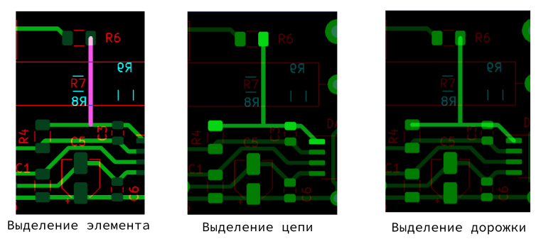
Selecting an element selects only one segment of the track we clicked on. Selecting a circuit selects the entire track and all the contact pads that the circuit includes. Track selection (called polyline in the program) excludes contact pads from selection. But the selection of colors of selected elements is a problem... First of all, for some reason, the selection is of different colors, and this cannot be changed, the color is selected automatically. Secondly, in some cases, when the selection is marked with the brightness of the same color, the contrast of the selection is frankly weak.
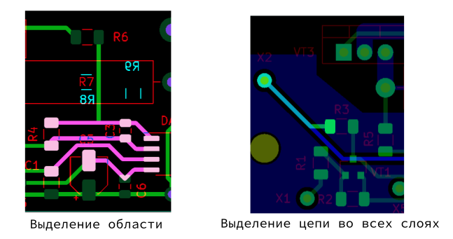
Selecting an area is a bit more complicated. The first click sets the first point of the rectangle's bounding area. The second click specifies a second point located diagonally to the first. All elements that are completely inside the selection area are considered selected. Selecting a circuit in all layers allows you to select, and thus verify the integrity of a circuit located in several copper layers and connected by transition holes or component pins. The illustration does not show this very well, but the tracks on both copper layers and the contact pads of the circuit are highlighted. You can clearly see that the automatic selection of highlighting colors is a bit strange.
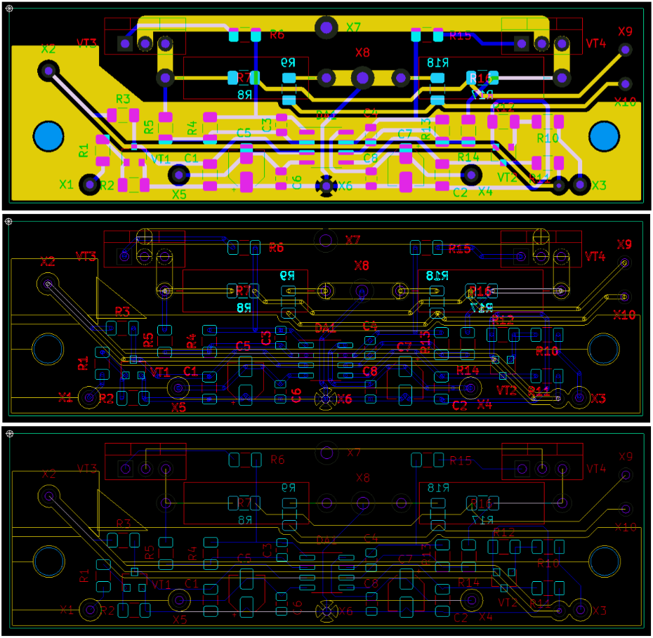
But this is not all the possibilities. Even the ability to turn off layers, change their color, and highlight elements does not always allow you to see the board well. And that's where the ability to change the display modes comes to our aid. This is done with the "F" key. You can also use the menu, but the hotkey is faster. I'll just give you different display options
If you want to see a more realistic view of the board, you can press the "Real View" button
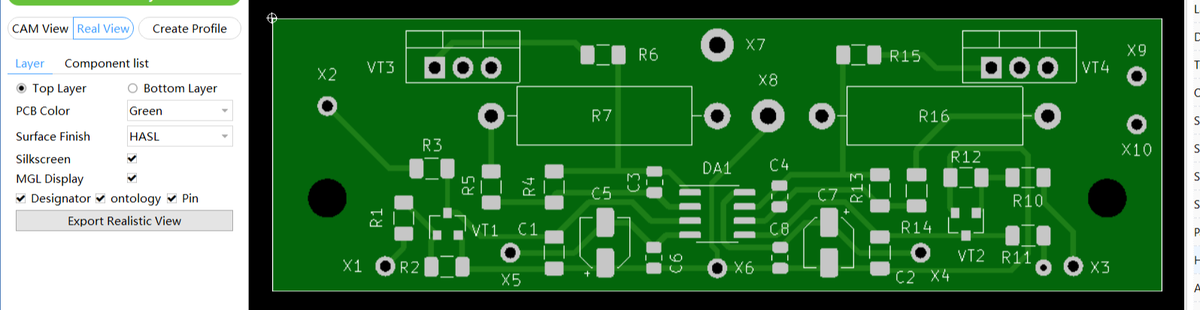
So, we can really look at our PCB in detail, using the manufacturer's tools and the way the manufacturer sees it. Yes, in KiCad we can also look at everything in detail. I already gave an example when everything was displayed correctly in KiCad, but the manufacturer interpreted Gerber files completely differently.
Besides, if the board was not developed by us, we will have only Gerber files, and not the full project, for example, KiCad. Therefore, I repeat, the possibility to look at the board through the manufacturer's eyes is useful.
But just seeing what the board looks like through the eyes of the manufacturer is not enough. It is much more important to find possible errors. Let me remind you, that we are using a set of Gerber files with errors so far. Let's go back to "CAM View" mode and press the big green button "DFM Analysis" (it is above the list of layers). After a short time, we will be notified that the analysis has been successfully completed.
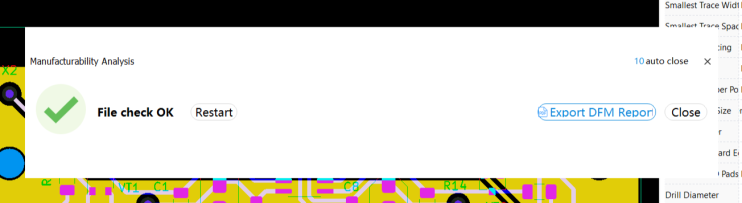
This window will automatically close after 10 seconds. And this is good, as there is a "spoon of tar" here as well. With each subsequent analysis, without restarting the program, this joyful window will get bigger and bigger, and will even exceed the screen size! If it didn't close automatically, we wouldn't be able to do anything, because the close button will be simply inaccessible (it will be outside the screen boundaries).
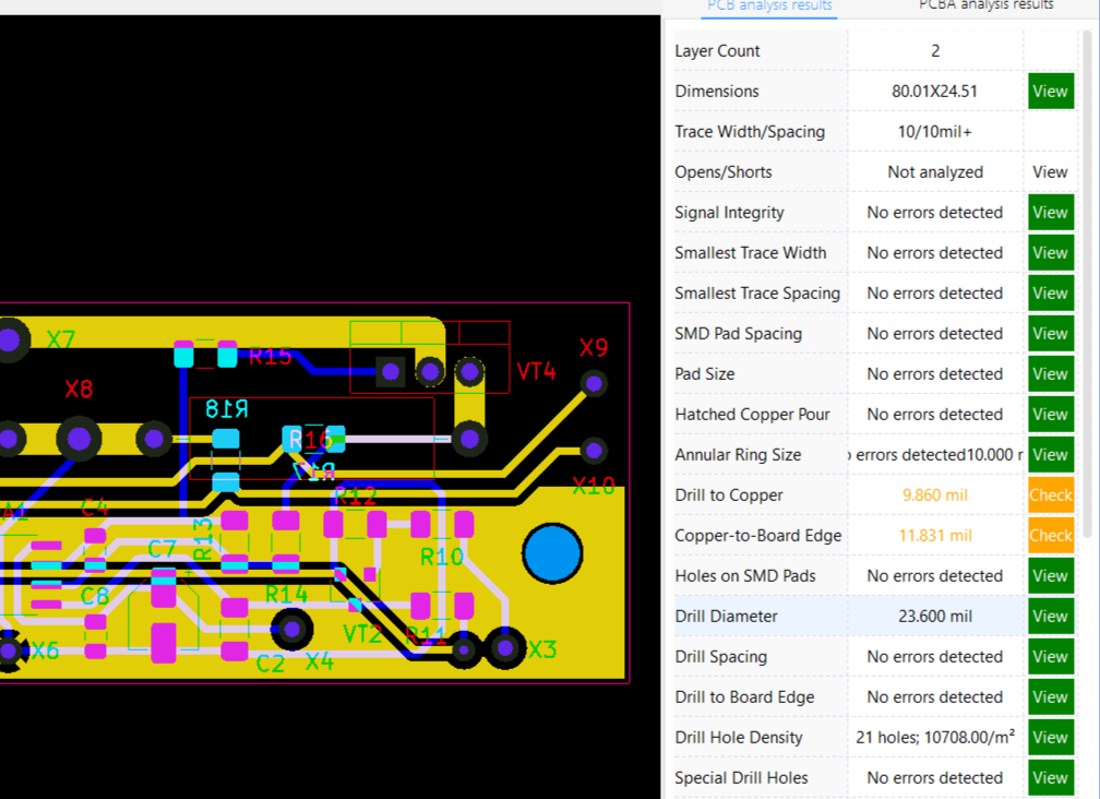
But let's look at the right part of the program window, where the rules are checked and the results of the check are displayed.
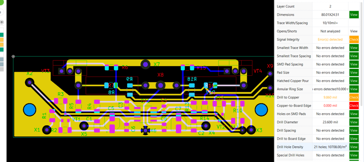
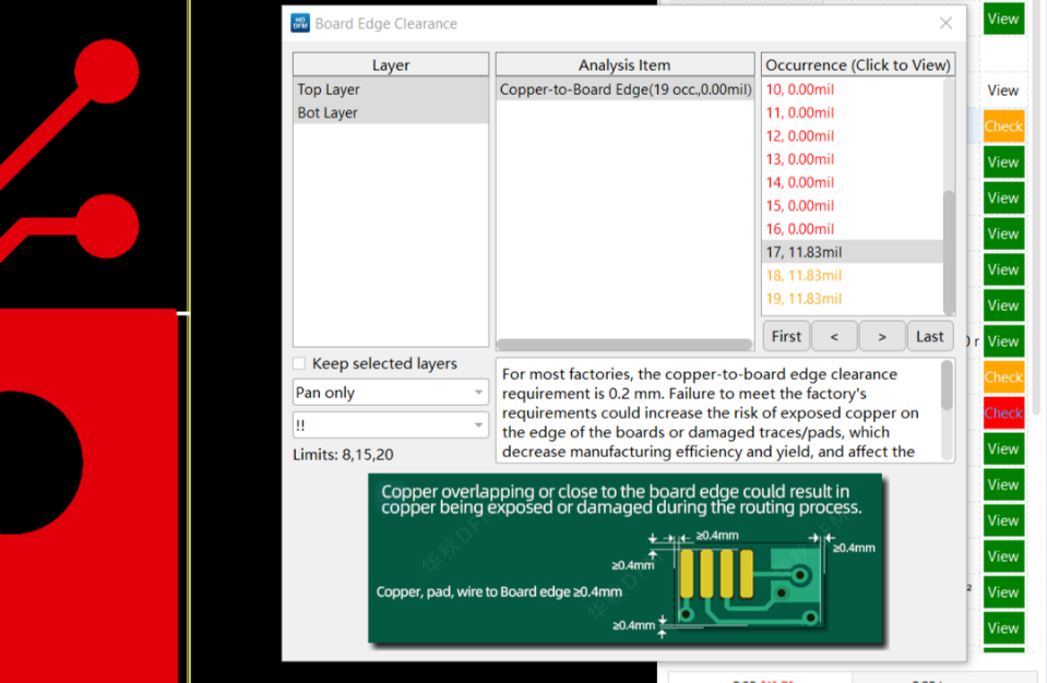
We can see that we have both errors shown in red and warnings shown in orange. But now, unlike NextPCB Online Gerber Viewer, we can see the error locations as well. Let's click on the red rectangle labeled "Check" under "Copper-to-Board Edge". We will see a window with a list of problematic locations related to this check.
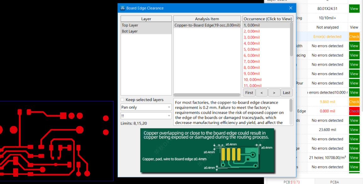
Not only the problem places are listed here, but there is also a description with an illustration. Therefore, you don't have to look at the "PCB Capabilities" page. When you click on any line in the "Occuremce (Click to View)" window, the error point is displayed in the middle of the board viewing area. I chose the "Pan only" mode to keep the scale of the board display unchanged. The window with the list of problem points can be moved by the mouse behind the header, which is what I did. This is what was missing in NextPCB Online Gerber Viewer.
And we can see here not only errors but also warnings. You can move and zoom the image of the board to get a better look at the error. Here is an example with a warning, where I have zoomed the image of the problem area
This small white line from the ground polygon to the right border is the problem spot. What these errors are, we have already discussed in detail in the previous article, so I won't repeat myself today. But you should agree that it is much easier and more convenient not to search for a point by coordinates in KiCad Gerber Viewer, but to find it immediately by clicking the mouse. We can easily find places that cause warnings, not errors. Let's click on the orange rectangle labeled "Check" in the "Drill to Copper" row.
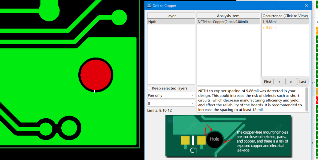
Unfortunately, there is a spoon of tar here too. Let's try to understand the "Signal Integrity" warnings. We will see a list of 6 errors, but no problem spot will be highlighted on the board image by clicking on it. The board image will be moved in the window, but the problem points will not be highlighted. Only the board borders will be highlighted. And the description with the illustration doesn't help, since there are no sharp corners in the center of the display area. In fact, this warning also occurs because of the Edge. The cut layer is displayed on all layers; we have already analyzed it in the previous article. But we didn't manage to show it visually in the program.
But let's load the Gerber files that fix the error with Edge. Cuts layer output on all layers. Just like we did in the previous article. Just like last time, no errors will be detected, but the warnings will remain, we didn't fix them
The "Signal Integrity" warning has disappeared as well, because of the error with Edge. The cuts have been fixed. The warnings with the distance between copper and drilling (fixing holes), which we have already disassembled last time, and the distance between the ground polygon on the bottom copper layer and the edge of the board, which we also have already disassembled.
When working with the program, the DFM inspection report file is not as necessary as when using NextPCB Online Gerber Viewer, but it can be generated via the menu "File -> Export Analyze Report". In doing so, it is completely identical to what we have already seen in the previous article. And since it is, we don't need to look at it again.
Studying the program features would be much easier if there was documentation available. Through the menu "Help -> Video Tutorial" you can find 13 tutorial videos, which is good. However, there are no text explanations or voice explanations (at least in English) in these videos. There is only a recording of working with the program. And this is already bad. But another thing is much worse: in the menu, there is an item "Tutorials -> Help Documentation", which opens the documentation file, but this documentation is in Chinese. The path to the file contains "HQDFM_en", which implies English. So the documentation, which is not bad, turns out to be completely useless.
The HQDFM Analysis Tool PC program is indeed much more functional than NextPCB Online Gerber Viewer. Despite the fact that we have not fully considered its capabilities. It allows you to not only examine the board in detail, and from the manufacturer's point of view but also to find problem areas, without resorting to other tools and without using an unfortunate and inconsistent report file. Naturally, you will still have to go back to KiCad (in our case) to fix the problems. But it is convenient to use the program.
And the general impression of the program is contradictory, but not negative. Yes, it is convenient and functional, but there are inexcusable errors. For example, the window with the notification about the analysis completion increases in size up to absolutely gigantic dimensions at each analysis start. There are some flaws, for example, color fiddling when working with layers and selections. One cannot ignore the absence of error messages from the installer, although the installed program turns out to be completely inoperable. Even under Windows on a real PC. And the documentation is only in Chinese, although the path to it implies English.
So the impression is contradictory-positive. If the developer of the program fixes at least the most annoying errors and flaws, the program will be certainly useful and convenient. From my point of view, which may not coincide with the readers' point of view.
you may also be interested in....
Still, need help? Contact Us: support@nextpcb.com
Need a PCB or PCBA quote? Quote now


 Surface

