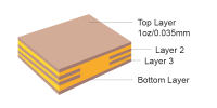
| Layer count |
1 - 32 layers |
Supports multilayer PCB manufacturing up to 32 layers, including advanced structures like
32L
HDI/Rigid-Flex Support, suitable for high-density applications |
/ |
| Impedance |
For 4, 6, 8, 10, 12, 14, 16, 18,
20 layers PCB,
PCB Stackup designed by
NextPCB(by default), or PCB Stackup
designed by customers
|
Standard pcb design for manufacturing flow includes impedance calculation based on default or
customer-provided stackups. Ideal for RF/high-speed signal applications.
|
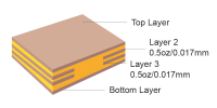
Layer Stackup Structure
Impedance Calculation Parameter
|
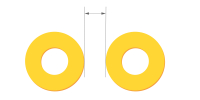
| Impedance tolerance |
±10% |
Ensures signal integrity in impedance-controlled PCBs for high-frequency applications |
/ |
| Material |
FR-4 |
Multiple Tg options available: TG130 / TG150 / TG170. These material options enable flexible
pcb
prototype fabrication service from standard to high-performance needs |
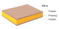 |
| PCB material dielectric constant |
4.2 |
Based on prepreg types: 7628 / 1080 / 2313 / 2116. Dielectric stability is critical for RF
and
signal-controlled PCB applications |
/ |
| Max. dimension |
1-2 layers: 1500*600mm
4 layers: 1500*500mm
6+layers: 500*400mm
|
Reflects NextPCB capabilities for large-format board manufacturing
|
|
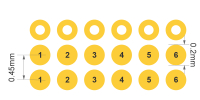
| Min. dimension |
≥10×10mm |
Suitable for small-format pcb prototype fabrication service, particularly useful in compact
consumer electronics |
/
|
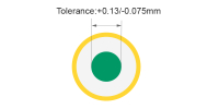
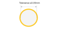
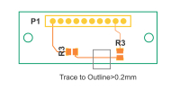
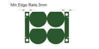
| Dimension tolerance |
CNC: ±0.15mm, V-CUT: ±0.2mm |
Tight pcb tolerances ensure outline precision and reduce post-processing mismatch risk
±0.15mm for CNC routing,
±0.2mm for V-scoring
|
/
|
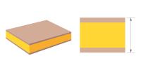
| PCB thickness |
0.6/0.8/1.0/1.2/1.6/2.0/2.5/3.0/3.2mm |
The thickness of finished board. This broad range meets standard and high-current carrying
PCB
applications. |
|
Thickness tolerance
( Thickness≥1.0mm)
|
±10% |
Enables accurate pcb manufacturing capabilities for multilayer boards
Example: If the board thickness is 1.6mm, the finished board thickness ranges from
1.44mm(1.6-1.6×10%) to 1.76mm(1.6+1.6×10%)
|
/
|
Thickness tolerance
( Thickness < 1.0mm)
|
±0.1mm |
Critical for thin board stackups in handhelds and flexible PCB applications
Example: If the board thickness is 0.8mm, the finished board thickness ranges from
0.7mm(0.8-0.1) to
0.9mm(0.8+0.1)
|
/
|
|
Finished copper weight
|
1 oz/2 oz |
Finished copper weight of outer layer could be 1 oz/2 oz
2oz copper thickness ensures high current capability and thermal performance in power boards"
|
|
|
Inner copper weight
|
0.5 oz/1 oz/2 oz |
Finished copper weight of inner layer could be 0.5 oz/1 oz/2 oz
Flexible copper distribution supports thermal design optimization and signal integrity
|
|
|
Surface finish
|
Multiple finishes to meet RoHS/REACH and solderability needs. Ideal for global PCB deployment
|
/
|
/
|
|
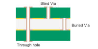
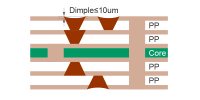
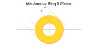
HDI structure
|
Rank 1 /Rank 2 /Rank 3 |
Advanced HDI options
Mechanical blind buried vias or laser blind buried vias(electroplating Via-filling is
available) or
laser blind vias filling dimple ≤ 15µm
Optimized for smartphones, wearables, and IoT boards"
|
/
|
|
Electrical test
|
Flying Probe/Special test fixture |
No pad count limits on flying probe. Fixture-based test supports up to 14,000 pads. Enables
strict
quality assurance in pcb manufacturer China standard
|
/
|
|
Beveling angle of gold finger
|
20°/30°/45°/60° |
Available for edge connectors in industrial and consumer hardware
|
/
|
|
Beveling angle tolerance of gold finger
|
±5° |
Ensures reliable mechanical contact and insertion accuracy
|
/
|
|
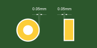
Beveling depth tolerance of gold finger
|
±0.1mm |
Precision control benefits connector mating and assembly yield
|
/
|
|
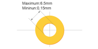
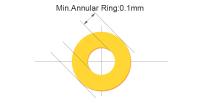
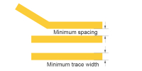
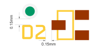
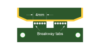
Outline tolerance
|
±0.15mm |
Supports CNC routing and tight-fitting mechanical enclosures
|
/
|
|
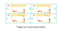
V-CUT angle
|
30°/45°/60° |
Various depaneling options suitable for volume pcb prototype fabrication service
|
/
|
|
Number of V-CUT
|
≤30 cuts |
Efficient for panelized delivery and cost-effective volume processing
|
/
|
|
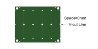
V-CUT outline size
|
55mm ≤ length/width ≤ 480mm |
Optimized for panelized batch manufacturing
|
/
|
|
V-CUT residue thickness
|
0.25mm ≤ v-cut residue thickness ≤ 0.4mm |
Balances structural integrity and ease of separation post-reflow
|
/
|

 NextPCB Capabilities
 PCB Assembly
 Layer Buildup
 SMD-Stencils
 PCB Design-Aid & Layout
 Mechanics
 Quality
 Drills & Throughplating
 Factory & Certificate
 PCB Assembly Factory Show
Certificate
PCB Assembly Factory Show
Certificate


 Surface