

 NextPCB Capabilities
 PCB Assembly
 Layer Buildup
 SMD-Stencils
 PCB Design-Aid & Layout
 Mechanics
 Surface
 Quality
 Drills & Throughplating
 Factory & Certificate


1. Understanding the Core: Surface Mount Technology (SMT) Explained
1.1 What is SMT? Defining Surface Mount Technology
SMT stands for Surface Mount Technology. Originally derived from short-lead flat mounting techniques used in US communication satellites, SMT technology experienced rapid development and maturation driven by the market demand for clearer picture quality in color televisions. Its accelerated growth was further propelled by the rapid iteration cycles of consumer electronics.
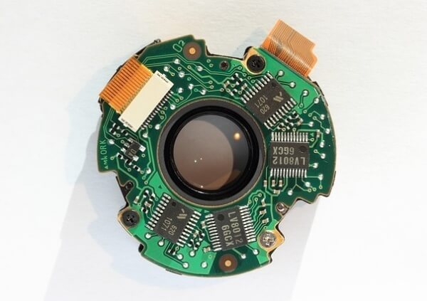
In modern PCB assembly, countless electronic components – smaller than grains of rice – populate the circuit boards inside your phone, computer, TV, and car. Precisely assembling these microscopic parts onto printed circuit boards (PCBs) is a fundamental process in electronics manufacturing, making Surface Mount Technology (SMT or surface mount technology) one of the most critical circuit board assembly techniques today.
Simply put, SMT meaning is: A board-level assembly technology that mounts Surface Mount Devices (SMDs) onto Printed Circuit Boards (PCBs). It is the cornerstone of modern electronics manufacturing. SMT is also commonly referred to as surface mounting technology or surface mount assembly.
1.2 The Hierarchy of Electronics Manufacturing: From Silicon to System
Understanding where SMT assembly fits requires knowledge of the tiered manufacturing process, known as Electronics Packaging Engineering:
- Level 0 Packaging: Creating the Core - Chip Level
- Output: Bare semiconductor die (often called a die or chip).
- Technology: Semiconductor fabrication.
- This foundational level produces the minuscule silicon "brains" of electronics.
- Level 1 Packaging: Protecting and Connecting - Component Level
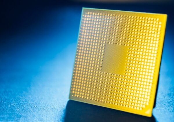
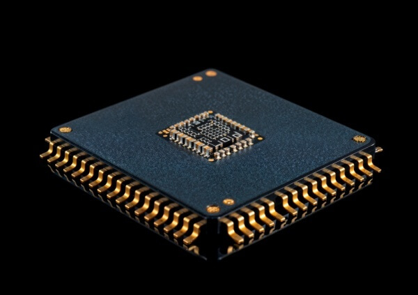
- Output: Packaged components (e.g., DIP, PLCC, QFP, BGA, QFN).
- Technology: Semiconductor packaging (e.g., wire bonding, flip-chip bonding).
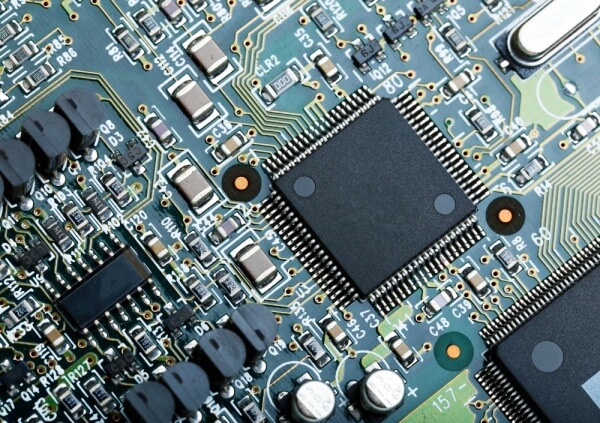
- Fragile bare dies are encased in protective packages with connection points (leads, balls, pads). Common SMT components or surface mount components like resistors, capacitors, and ICs in packages like BGA or QFN are results of this level.
- Level 2 Packaging: Building the Foundation - Board Level (SMT's Domain)
- Output: Printed Circuit Board Assembly (PCBA).
- Technology: Electronic assembly technology, primarily Surface Mount Technology (SMT) (e.g., solder paste printing, reflow soldering, wave soldering), sometimes including microassembly.
- This is where SMT manufacturing shines. Level 1 packaged components and other SMT electronic components are accurately placed and soldered onto a PCB (SMT PCB) or surface mount PCB. The result is a functional PCBA – the essential "foundational backbone" of the final product. SMT assembly services specialize in this step.
- Level 3 Packaging: System Integration - Product Level
- Output: Final electronic product.
- Technology: Backplane/wire/cable assembly, enclosure integration.
- Multiple PCBAs are interconnected using backplanes and harnesses, housed with screens, batteries, and enclosures to create the final device (phone, laptop, etc.).
Therefore:
- Electronic Interconnection Technology: Encompasses Level 2 and Level 3 packaging, focusing on connecting assemblies within the system chassis.
- Electronic Assembly Technology: Primarily refers to Level 2 packaging (PCBA creation). Its core function is reliably mounting and electrically connecting chips and components onto the circuit board. SMT is the dominant mainstream technology here, ideal for high-density micro-components, alongside specialized microassembly techniques.
1.3 The Advantages: Why SMT Dominates Electronics Assembly
Compared to legacy Through-Hole Technology (THT), SMT offers compelling benefits that revolutionized SMT production:
- Exceptional Component Density: SMT components use short leads or leadless designs (e.g., array packages like BGA). This miniaturization allows significantly more components on the same PCB area, enabling ultra-compact devices like smartphones.
- Enhanced Electrical Performance: Short/no leads minimize parasitic inductance/capacitance, boosting high-frequency/speed circuit performance and improving thermal dissipation.
- Lower Manufacturing Costs: Standardized component packaging and leadless (no-drill) assembly enable high-speed automation across the SMT line, dramatically reducing labor costs compared to manual THT.
- Increased Reliability: Automated, standardized processes deliver consistent, robust solder joints (PCBA quality), leading to more reliable end products.
These unparalleled advantages fueled SMT's global adoption and continuous advancement.
2. SMT Equipment & Process Flow Explained
2.1 Standard SMT Line Configuration
A typical SMT manufacturing line follows this sequence:
- Loader: Feeds blank PCBs into the SMT line.
- Solder Paste Printer (Surface Mount Machine): Precisely deposits solder paste (tiny metal spheres + flux) onto PCB pads using a stencil, much like screen printing. (Critical Step)
- Solder Paste Inspection (SPI - SMT Equipment): A high-speed camera system automatically checks paste deposit volume, shape, alignment, and height immediately after printing. Catches defects early.
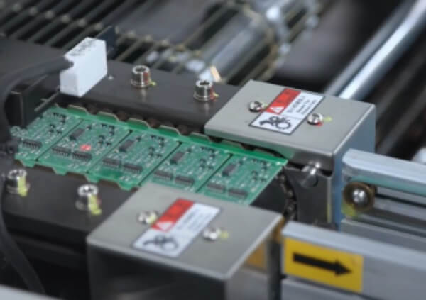
- Multi-Function Pick-and-Place Machine (SMT machine): High-speed, computer-controlled robots, equipped with tiny nozzles, pick surface mount components (SMDs) from reels/trays and place them with extreme precision onto the solder paste deposits. Speed & Accuracy are key.
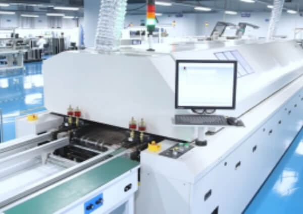
- Reflow Oven (Surface Mount Technology Machine): The populated PCB travels through a precisely controlled heated tunnel. A programmed thermal profile melts the solder paste, forming permanent solder joints as it cools. Essential for surface mount assembly integrity.
- Auto Optical Inspection (AOI - SMT System/Inspection Tech): Post-reflow, AOI scans the assembled PCB to verify component presence, placement accuracy, and solder joint quality (detecting shorts, opens, misalignments).
(Additional common steps: Loader/Unloader, potential board wash, functional test.)
How Does a High Precision SMT Line Work
2.2 The Core Pillars of SMT: Technology and Materials
Successful SMT assembly relies on four interconnected pillars:
- SMT Process Technology: The core. Encompasses everything needed for consistent production & quality:
- Component pad design on the SMT PCB.
- Solder paste stencil ("SMT Stencil") design & fabrication.
- Optimal machine programming (printer, SMT machine, oven).
- Reflow soldering profile ("temperature curve") definition & control.
- Production workflow design.
- Testing/Repair strategies.
- Fixture/tooling design for complex parts. (Crucial for yield)
- SMT Equipment Technology: The machines enabling automation - Printers, SPI, pick-and-place machines, Reflow/Wave Ovens, AOI, X-Ray.
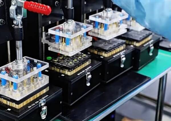
- Process Materials: Solder paste, fluxes, cleaners, adhesives, and the surface mount electronic components themselves. Material quality directly impacts yield.
- Inspection Technology: SPI, AOI, X-Ray, Functional Test - ensuring quality at each stage.
Optimization Insight: Successful SMT manufacturing often integrates Level 1 Packaging (component design) and SMT PCB design considerations. The synergy between component pad layout (package design), PCB land pattern design, and SMT processes/equipment is vital for manufacturability and reliability. The three domains evolve together, driving overall electronics manufacturing progress.
|
Category |
Sub-items |
|
Process Technology |
Pad Design, Stencil Design, Parameter Settings (Printing, Placement, Soldering Equipment), Reflow Oven (Heating Program Design, Temperature Profile), Assembly Flow Planning, Testing & Repair, Tooling & Fixtures |
|
Equipment Technology |
Solder Paste Printer, Solder Paste Inspection (SPI), Pick and Place Machine, Reflow Oven, Wave Soldering Machine, Automated Optical Inspection (AOI) |
|
Process Materials |
Solder Paste, Flux, Cleaning Agent, Adhesives, SMT Components |
|
Inspection Technology |
SPI (Solder Paste Inspection), AOI (Automated Optical Inspection), X-Ray Inspection, Functional Testing |
3. Why Process Technology is the Unbeaten Heart of SMT
Among the pillars, SMT Process Technology reigns supreme:
- The Ultimate Goal: Create reliable solder joints. Success hinges on correct PCB pad design (part of DFM), precise solder paste volume & placement, and an optimal reflow profile – all core process elements.
- The Differentiator: Factories using identical SMT equipment achieve vastly different yields. Why? Process mastery. Excellence demands:
- Scientific Methodology: Controls must be valid and effective. E.g., Measuring flux dip height on PoP (SMT Pop process) parts using a static hex comb gauge is common, but ignores the difference between static measurement and high-speed dynamic dipping during SMT mounting. The control exists on paper but doesn't translate to actual process control – lacking scientific rigor and effectiveness. If the target or method is flawed scientifically, control is meaningless.
- Precision & Detail: Steps require well-defined, measurable outcomes. E.g., Solder paste mixing instructions stating "mix 5 times" lack precision. Different operators achieve different viscosity/consistency. A robust process specifies a measurable target (e.g., viscosity range, homogeneity test result, or standardized mixing equipment parameters). This is precision.
- The Asset: Pad/Stencil design, machine settings, oven profiles, specialized fixtures – all captured in documented methods and rules – constitute the process. This codified knowledge, gained through years of experience and experimentation, is a manufacturer's most valuable asset (closely guarded!). It directly governs equipment utilization, process efficiency, and final product quality and reliability. It's why "Process Determines Equipment Effectiveness, Production Efficiency, and Product Quality."
> See How to Choose Reliable PCB Manufacturer form China
Mastering SMT process technology is the key differentiator for high-yield, high-quality circuit board assembly services.
Engineering Insight: At NextPCB, we engineer reliability from the ground up. Our ISO-certified SMT assembly lines don't just run – they're governed by proprietary process libraries refined through 3.2 million+ component placements.
3.1 Why NextPCB Unlocks Your Design Potential
- Scientific Process Control:
We maintain strict control over our solder paste printing, pick‑and‑place alignment, and thermal profiling to help optimize assembly yield.
- DFM & Online Tools:
Upload your Gerber file to our free HQDFM/DFM analysis tools with automated design rule checks and Gerber visualization.
- Prototype to Volume:
We support ultra-fine SMT (01005, 0.38 mm pitch ICs, BGA 0.25 mm), mixed SMT/THT boards, express delivery options (as fast as 24 h), and flexible BOM procurement.
>> If you are evaluating manufacturing vendors for your next hardware spin, check out our comprehensive NextPCB vs JLCPCB vs PCBWay comparison guide.
Ready to Start?
- Upload your design now to get an instant DFM check and quote via our HQDFM Gerber Viewer.
- Need rapid turnaround? Ask about our 24h express assembly service.
- Curious about our facility? Contact us to schedule a live or virtual factory tour.
For prototypes to volume runs – Your process edge starts here:
You may also insterested in:
PCB Assembly - The Most Comprehensive Guide | NextPCB
What is the difference between SMT and SMD?
SMT Red Glue: Why It's Used & How to Optimize for Cost-Effective PCB Assembly

