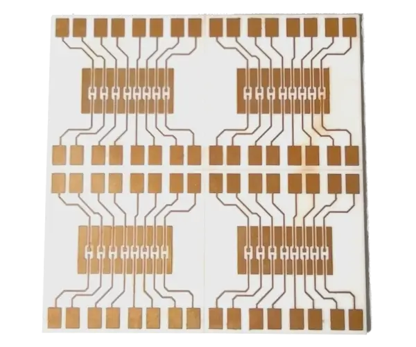
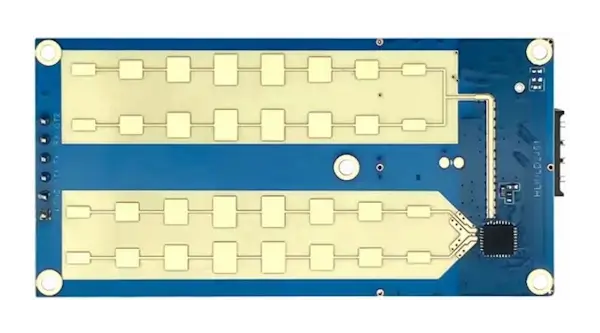
The diverse range of properties exhibited by ceramic materials has enabled their adoption as PCB substrates, surpassing conventional fibreglass epoxy and metal options in high-performance electronics. These Ceramic PCBs have allowed engineers to push the boundaries with their superior thermal management, high-frequency performance and durability.
NextPCB offers ceramic PCBs suitable for the most demanding high-performance applications from aerospace to high-frequency electronics. Choose from standard Aluminum Oxide and Aluminum Nitride substrates or specialty ceramics, and DBC, DCP and AMB technologies for optimal performance in the harshest environments.
What are Ceramic PCBs?
Ceramic PCBs use ceramic materials; metallic oxides, nitrides, carbides or crystalline silicon and carbon structures as their base. Unlike metal-core PCBs, the high electrical insulating properties of ceramic substances mean no dielectric layer is required to isolate the copper from the substrate, allowing for more efficient thermal transfer. Challenges in fabricating ceramic PCBs mainly reside in forcing copper to bond to the crystalline structure reliably while optimizing the desired properties, giving rise to advanced techniques.
>> Recommend: Advanced PCB Capabilities - NextPCB

Advantages of Ceramic PCBs
The crystalline structures of ceramic materials impart the defining properties associated with ceramics, such as high hardness, low electrical conductivity, and exceptional wear/chemical resistance. These properties allow them to outperform metal-core PCBs in mechanical stability and long-term durability while matching or surpassing their thermal management capabilities. In this section, we go over the key advantages of ceramic materials as PCB substrates.
High Thermal Conductivity
High thermal conductivity gives ceramic substances superior heat transfer and dissipative properties compared to fibreglass materials. For example, alumina PCBs have 50x better heat dissipation compared to FR4 PCBs. In addition, the absence of a dielectric layer and innovative techniques such as PCB-on-Heatsink, where the circuitry sits directly on top of a heatsink-shaped ceramic substrate, allow for even greater thermal performance.
| Bare Material |
Thermal Conductivity (W/mK) |
Advantages |
| FR4 |
0.2-0.5 |
Multilayer, dense circuitry |
| Aluminum (Al) |
140-180 |
Lightweight, high thermal conductivity |
| Copper (Cu) |
385-400 |
Ultra-high thermal conductivity |
| Alumina (Al2O3) |
18-35 |
Most common ceramic substrate, cost-effective, all-around performance |
| Aluminum Nitride (AlN) |
140-180 |
High thermal conductivity, strong electric insulator, low CTE |
| Silicon Carbide (SiC) |
120-200 |
High resistance to thermal shock |
| Silicon Nitride (Si3N4) |
20-95 |
Good balance of thermal, electrical and mechanical properties |
| Zirconia (ZrO3) |
2-3 |
Thermal insulating properties |
| Sapphire (Al2O3) |
25-40 |
Transparent, low surface roughness, good for optics |
| Diamond (C) |
1400-1850 |
Exceptionally high thermal conductivity |
Strong Electric Insulator
Ceramic materials are naturally excellent electrical insulators, which gives them the edge over insulated metal substrates (IMS). From the table above, one might assume that metallic bases offer the best heat dissipation. However, IMS PCBs have a dielectric layer separating the circuitry from the metal base, limiting thermal conductivity to around 10W/mK. For ceramic substrates, the traces are printed directly on the substrate, allowing for thermal conductivities to easily reach over one hundred W/mk.
High Mechanical Strength and Durability
Resistance to warping and high hardness are typical traits of ceramics. In addition, ceramic materials are resistant to thermal shock, wear and chemical corrosion and can withstand extreme temperatures, making them ideal for demanding environments such as aerospace, military, and industrial applications.
Low Dielectric Loss
Ceramic PCBs maintain low dielectric constant (Dk) and low dissipation factor (Df) even at high temperature and frequency, making them ideal for high-frequency, high-speed, and high-power applications such as high-frequency RF/mmWave circuits and ultra-low-loss components.
When to Choose Ceramic PCBs?
From the section above, it is clear that ceramic PCBs have a significant set of advantages that make them worthy of serious consideration for numerous high-power applications, replacing metal-core PCBs in many cases. However, due to the high production costs and limitations, ceramic PCBs may not be the ideal solution for certain applications.
- No.of Circuit Layers: Ceramic PCBs using copper bonding technologies, similar to metal-core PCBs, are limited to single and double-sided configurations, limiting circuit density. Multilayer and 3D structures are possible; however, this comes at the expense of thermal conductivity, stability and cost.
- High Production Costs: The main advantage of ceramic PCBs comes from their exceptionally high thermal management properties. However, the high cost of these PCBs may make IMS solutions more favorable for less demanding and cost-sensitive applications.
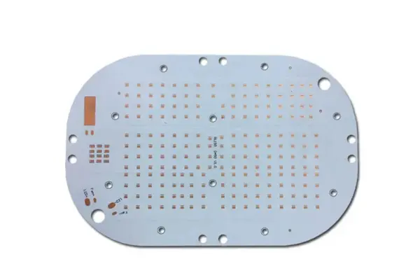
- Size: Due to the brittleness of ceramic materials, ceramic PCBs are typically limited to small dimensions within 150 x 150mm, making them unsuitable for larger designs. Ceramic PCBs excel with compact and simple designs, for example, medical implants and power modules.
If space, thermal management and reliability are not constraining factors for your design, consider IMS metal-core solutions and pedestal technology.
>> Recommeng reading: Ceramic PCB vs FR4 vs Metal-Core: Substrates for Thermal Management
NextPCB Ceramic PCB Manufacturing Capabilities
| Feature |
Specification |
| Structure |
- Single-sided, double-sided, multilayer
- Direct Plated Copper (DPC) or Direct Bonded Copper (DBC)
|
| Base Material |
Standard:
- Aluminum oxide (Al2O3 96% and 99%)
- Aluminum nitride (AlN ≥170 and ≥230 W/mK)
Specialty Materials:
- Silicon carbide (SiC)
- Silicon nitride (Si3N4)
- Zirconia (ZrO2)
- Diamond (C)
- Sapphire (Al2O3 single-crystal alumina)
- Polycrystalline silicon wafers
See table for more
|
| Max Dimensions |
120 x 120mm |
| Board Thickness |
0.1 to 3.0mm |
| Circuit Layers |
1 or 2 layers, inquire for more |
| Copper Thickness |
1-1000μm (~30 oz) |
| Min. Trace width/spacing |
2/2 mil |
| Drill and Via Capabilities |
- Round and square plated holes and slots
- Electroplated and filled vias
- Half-hole (castellated holes), side-plating
|
| Min. Drill Hole Diameter |
0.05 ±0.025mm |
| Surface Finish |
Immersion silver, ENIG, ENEPIG or OSP |
| PCB Solder Mask Color |
Green, blue, white and black |
| Extras |
- Impedance control
- Peelable solder mask
- Carbon ink
- And more
|
| Industries & Applications |
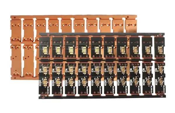
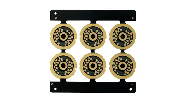
- Smart Lighting: High-power LED modules, COB LEDs
- Biomedical: Implantable sensors, biomedical testing
- Renewable Energy: PV inverters, high-temperature sensors
- Telecom & 5G: RF amplifiers, microwave circuits
- Power Electronics: IGBTs, MOSFETs, power converters
- Automotive Electronics: BMS, inverter modules
|
| Certifications |
ISO9001:2015
ISO14001:2015
|
Inquire for a quote now
NextPCB Ceramic PCB Materials
NextPCB supports a variety of HTCC ceramic substrate materials for both common and advanced niche applications. Below are the properties of some of NextPCB's supported ceramic substrates.
Aluminum Oxide (96%)
Al2O3 |
Aluminum Nitride (96%)
AlN |
Silicon Carbide
SiC |
Silicon Nitride
Si3N4 |
Zirconia
ZrO2 |
Zirconia-Toughened-Alumina (ZTA) |
Sapphire
Al2O3 |
Diamond |
| Bulk Density (after sintering) |
g/cm3 |
≥ 3.7 |
3.33 |
3.1-3.15 |
≥ 3.22 |
≥ 6.0 |
≥ 4.10 |
≥ 3.86 |
3.42-3.52 |
| Warpage |
% |
≤ 2 |
≤ 2 |
≤ 2 |
≤ 3.18 |
≤ 4 |
/ |
/ |
/ |
| Surface Roughness |
μm |
0.2 ~ 0.75 |
0.2 ~ 0.6 |
0.2 ~ 0.4 |
0.2 ~ 0.4 |
0.1 ~ 0.2 |
0.1 ~ 0.2 |
0.05 ~ 0.08 |
0.02 ~ 0.002 |
| Thermal Conductivity (20°C) |
W/mK |
≥ 24 |
≥ 170 |
≥ 100 |
≥ 20 |
≥ 3 |
≥ 27 |
≥ 26 |
1400 - 1850 |
| Coefficient of Thermal Expansion (CTE) |
ppm/°C
x 10-6/K |
4.5 ~ 8.0 |
2.0 ~ 3.5 |
4 |
3 |
7.8 |
8 |
7.2 |
1 ~ 1.5 |
| Dielectric Constant (1MHz) |
- |
9 ~ 10 |
8 ~ 10 |
/ |
8 ~ 10 |
33 |
10.4 |
9.6 ~ 10.2 |
5.6 |
| Dielectric Strength |
KV/mm |
≥ 17 |
≥ 17 |
/ |
1014 |
≥ 10 |
≥ 10 |
/ |
≥ 10 |
| Volume Resistivity |
Ω·cm |
≥ 1014 |
≥ 1013 |
/ |
≥ 1014 |
≥ 1013 |
≥ 1014 |
≥ 1014 |
≥ 1014 |
| Flexural Strength |
MPa |
≥ 350 |
≥ 330 |
≥ 400 |
≥ 980 |
≥ 800 |
≥ 650 |
≥ 550 |
≥ 450 |
| Color |
- |
White |
Grey |
Grey |
Grey |
White |
White |
Clear |
Pale Yellow |
Get in touch for more details or a quotation
FAQ
What is the difference between LTCC and HTCC ceramic materials?
LTCC (Low-Temperature Co-Fired Ceramic) materials are known as glass-ceramics and HTCC (High-Temperature Co-Fired Ceramics) are known as pure-ceramics for their ceramic content and production process. LTCCs are fired with glass-ceramic additives to lower the sintering temperature from 1500-1600°C to around 850-950°C. This reduces cost and production time, making them suitable for prototyping, RF applications and creating 3D structures; however, they do not have nearly as high thermal conductivity or mechanical strength as pure-ceramic compositions.
At NextPCB, we use pre-fired high-temperature ceramic substrates and advanced technologies to bond conductive metals to the surface of ceramics instead of firing them from scratch. This allows us to use high-conductivity copper for the circuitry (instead of tungsten/molybdenum) and reduce production lead times and cost, while retaining the high thermal conductivities and properties of HTCCs.
How are Ceramic PCBs made?
We use advanced DBC (Direct Bonding Copper), DPC (Direct Plating Copper) and AMB (Active Metal Brazing) technologies to force strong bonds between metal ions and the surface of various ceramic materials. Due to ceramics' inert and non-reactive nature, high temperatures, interface materials and strict environmental conditions are required to achieve heterogeneous bonding. Each technique has its advantages and disadvantages:
DPC (Direct Plating Copper): The direct plating copper thin film process is similar to the plating process for FR4 epoxy printed circuit boards. Magnetron sputtering technology is used to coat surfaces with a uniform interface layer consisting of tin and copper. The interface layer makes it easier for copper to attach, allowing for electroplating to build up copper thickness and plate holes. Copper elements are then etched out with standard lithography and etching processes. The DPC technique is a versatile method that allows for more precise circuitry than other methods and is well suited for plating through-holes and vias.
DBC (Direct Bonding Copper): Direct bonding copper technology sinters copper foils directly onto the surface of ceramic substrates using a high-temperature oxidation process. At 1065-1083°C, a copper-oxygen eutectic forms, which bonds to both ceramic oxides and copper. Circuitry can then be etched using standard processes. This technology is suitable for PCBs requiring high copper thicknesses up to 10oz heavy copper.
AMB (Active Metal Brazing): The AMB technique uses active solder paste, or brazing material, consisting of active elements such as tin and zirconium to increase wettability. When heated to 800°C, they form a heterogeneous metallurgical bond between the ceramic and copper surfaces. The result is a copper-clad ceramic substrate with high mechanical strength, thermal shock resistance and excellent thermal conductivity. Silicon Nitride (Si3N4) PCBs produced using AMB technology have much higher thermal conductivity (90W/mK) compared with Alumina (Al2O3) PCBs made with other methods and have a CTE value close to silicon.
How are Ceramic PCBs cut out?
The profiles of ceramic PCBs, including drill holes, are cut using high-power precision lasers such as fiber lasers. Despite their high mechanical strength, ceramic materials are inherently brittle. Drilling and milling methods can cause ceramics to chip, crack, or result in excessive tool wear.
Can you make ceramic PCBs with plated through holes?
Yes, the DPC process is highly suited to producing ceramic PCBs with plated holes and interconnects for a wide range of ceramic materials. For heavier copper weights and requirements, get in touch to find out more.

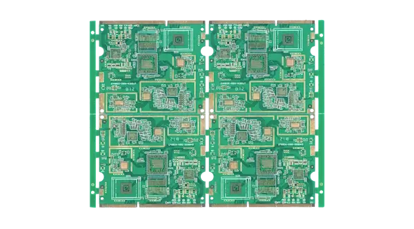
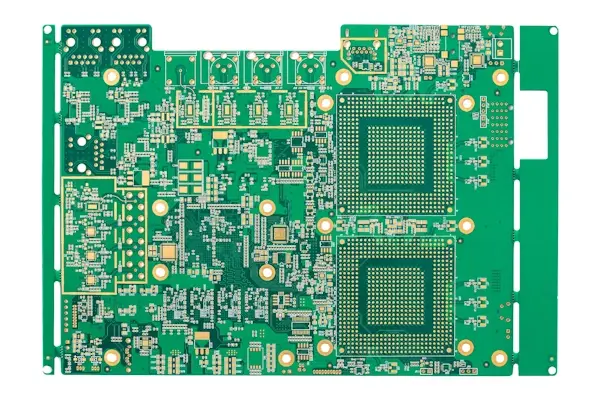
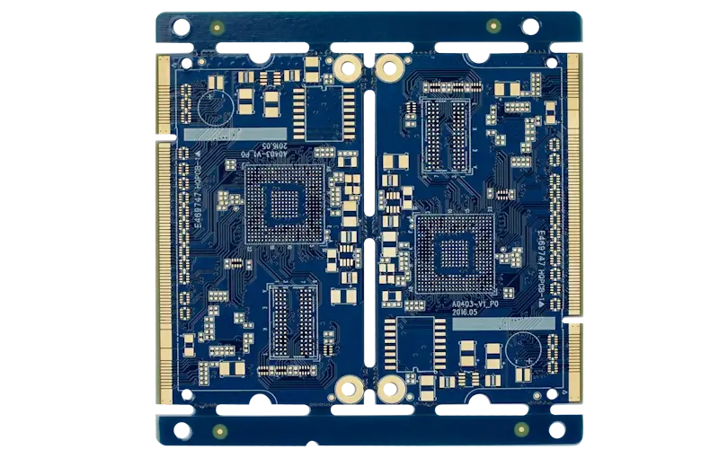
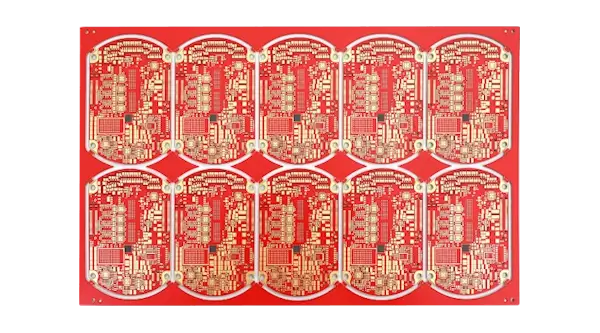
 NextPCB Capabilities
 PCB Assembly
 Layer Buildup
 SMD-Stencils
 PCB Design-Aid & Layout
 Mechanics
 Surface
 Quality
 Drills & Throughplating
 Factory & Certificate