Side plating
Posted: 09:49 AM December 25, 2019
writer: NextPCB
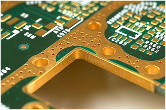
Side plating also called edge plating, border plating, or side metal. It means that the edge of the board is metalized. In other words, side plating is the copper plating that runs from the top to the bottom surfaces of a board and continues one or more perimeter edges. Both partial outline of the board and the partial areas in the board can be metalized.

The process of side plating or edge plating
Although side plating on PCBs is a simple technology in most cases, PCB manufacturers need trained personnel and specialized equipment for the process.
First, PCB designers need to take care that the internal power layer does not reach the edge, and ensure the copper strips exist on both edges of the top and bottom sides because the plating will connect to these copper strips.
Second, PCB manufacturers must guarantee that there is a gap before performing side plating. Besides, side plating requires precise handling of the board. The main challenge for manufacturers is to prepare the edge of the plating and create lifetime adhesion for the material of side plating. And the most significant is to prevent the creation of burrs, which will cause the failure of critical parts and limit the adhesion life of the side plating.
The functions of the side plating
Side plating provides measurable benefits for the devices with moderate or high demands in EMC, heat dissipation, signal-integrity, strong connection, etc. The main functions are listed below:
- Support better connections, such as the boards need slide into metal casings
- Improve the EMC behavior by shielding the edges of the multi-layer PCB
- Better performance in heat dissipation as the edge is the additional cooling surface
- The advantage for signal-integrity inn the point of signal transfer from device to the periphery
- Prevent electromagnetic emissions from radiating or leaking out of the edge of the backplane.
- Improve the current-carrying capabilities of the board
- Provide the edge connection and protection
- Offer the possibility of edge soldering to improve manufacturing
Design parameters of the side plating
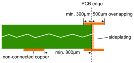
To be productive of the side plating, it is necessary to use overlapping metal (copper surface, pad, or tracks) in the CAD layout to define the metalized area.
On the connected layer, a minimum of 300μm of connecting copper must be defined.
On non-connected layers, the distance between copper and the outer contour should be at least 800μm.

Customers must confirm the capability of fabricating PCBs with side plating with PCB fabricators if having the requirement of side plating, and customers should indicate the type of side plating and the surface finish in the mechanical layer clearly. Engineers in NextPCB usually recommend customers use ENIG or immersion silver for the side plating of PCBs. NextPCB has rich experience in PCB manufacturing with the requirement of side plating. Please do not contact the online service or send Emails to support@nextpcb.com if you need more technical details about the side plating process and specifications.
 PCB Assembly
 Layer Buildup
 Online Tools
 PCB Design-Aid & Layout
 Mechanics
 SMD-Stencils
 Quality
 Drills & Throughplating
 Factory & Certificate
 PCB Assembly Factory Show
Certificate


