A pillar guide to principles, pros/cons, standards, and deployment
Introduction: This page organizes PCB/PCBA quality verification by test category. For each category you’ll find the method, how it works, core benefits and trade-offs, typical use cases, and commonly referenced standards. Use it to design a right-sized test strategy from prototype to mass production.
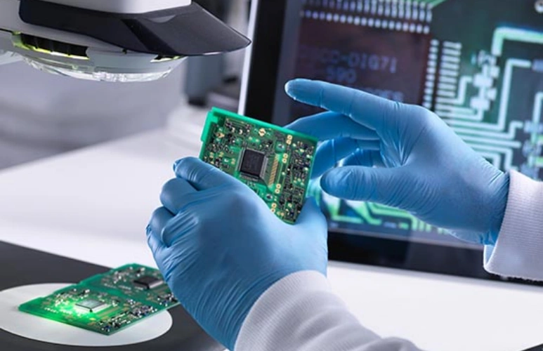
From 3D SPI/AOI to AXI, ICT, and reliability runs, NextPCB delivers the right test stack for your design, quantity, and budget. Upload your files and get a fast, engineer-reviewed quote.
Definition: PCB testing is the staged verification of bare boards and assembled PCBAs to prove design intent, electrical safety, and long-term reliability from prototype through mass production. It’s not one tool but a layered stack you right-size for risk, volume, and budget—catching issues as early (and cheaply) as possible while maintaining diagnostic depth.
At a glance, the stack:
Non-contact inspection to stop print/placement defects early (e.g., SPI, AOI).
Electrical coverage to find opens/shorts and part faults (bare-board E-test, Flying Probe, ICT, Boundary-Scan).
Hidden/structural checks for BGAs, vias, and laminates (AXI, C-SAM, microsection).
Reliability & domain-specific validation (SIR/CAF, thermal cycling/shock, TDR/insertion loss for high-speed, HiPot/IR for safety) plus mechanical controls (warpage/coplanarity, profilometry).
Use this guide to choose the minimum-viable set that balances coverage, diagnostic power, cycle time, and fixture cost for your design.
1. Optical & Visual Inspection
Optical inspection looks for visible defects before they become electrical failures. It ranges from manual checks with a loupe to automated optical inspection (AOI) that compares camera images to a golden reference. Modern 3D AOI also measures height/volume, so it can spot tombstoning, polarity errors, and insufficient solder more reliably than 2D. It’s fast, non-contact, and ideal for early, high-throughput screening.
Structured light/Moiré height map; reconstructs joint and component geometry
Quantifies height/volume; robust on tombstoning, polarity, misorientation; great with SPI data
Higher capex; tuning required
Primary station for mid/high-density SMT lines
Takeaway: 3D AOI is becoming mainstream; pairing SPI → AOI creates a closed loop to stop defects early.
2. Pre-print / Solder Paste Inspection (SPI)
Most SMT defects start at the stencil printer, so SPI measures the volume, height, area, and offset of solder paste on each pad. By catching underprint, bridging risk, or misalignment before placement, SPI prevents expensive downstream rework. The data also feeds process control (SPC), helping tune printer parameters and stencil designs. For fine-pitch parts (0201, BGA/QFN), SPI is a must-have gate.
Solder paste inspection methods
Method
How it works
Strengths
Limitations
Typical use / Standards
3D SPI
Structured light or laser scan of volume/height/area/offset on pads
“Gate #1” before reflow; strong predictors for bridges and insufficient paste; data-driven SPC
Electrical tests prove that the board isn’t just pretty—it actually works. Flying Probe is fixture-less and flexible for prototypes, while ICT uses a bed-of-nails for fast, parallel coverage in mass production. Boundary scan (JTAG) reaches dense or hidden nets without probes, and FCT powers the board in realistic conditions to catch system-level issues. Together they balance coverage, speed, and cost across the product lifecycle.
Scan chain tests interconnects among scan-capable ICs
Fixture-less access to dense/hidden nodes; complements ICT
Requires scan-enabled devices and test vectors
High-density digital boards; mixed strategy with ICT
4. Internal Structure (NDT & Destructive)
Some faults hide inside the board or under components. AXI X-ray reveals voids and bridges in hidden joints like BGA, while C-SAM ultrasound detects delamination and voids in laminates and packages. When root cause demands it, microsectioning cuts and polishes a small coupon to show vias, copper thickness, and resin flow directly. NDT preserves the product; destructive analysis delivers the most detail.
Direct view of via copper, resin flow, layer registration, inter-laminar issues
Destructive; cycle time
Process validation and failure analysis (IPC-TM-650 family)
5. Surface Finish, Plating & Solderability
Surface finishes (ENIG, ENEPIG, etc.) and plating quality drive both reliability and appearance. XRF quickly and non-destructively measures coating thickness and alloy ratios to verify process control. Solderability tests quantify how well pads wet with a given alloy, especially after storage or finish changes. These checks reduce risks like black pad, poor wetting, and early field failures.
Flux residues and trapped ions can trigger electrochemical migration, corrosion, or leakage over time. ROSE gives a fast read on total ionic residues for day-to-day process monitoring, while ion chromatography identifies the exact contaminants during investigations. Cleanliness matters most for high-impedance, high-reliability, or harsh-environment products. Keeping residues in control extends lifetime and reduces intermittent field issues.
Reliability tests accelerate real-world stresses to expose long-term risks. SIR evaluates insulation behavior under heat, humidity, and bias; CAF checks whether conductive filaments may form within the laminate; thermal cycling/shock probes solder and interlayer fatigue. These methods validate new materials and processes, and they’re standard for automotive, medical, and aerospace. The goal is predictable lifetime, not just day-one pass.
Reliability and environmental stress methods
Method
How it works
Strengths
Limitations
Typical use / Standards
SIR
Monitors surface insulation resistance under temperature, humidity, and bias
Evaluates ECM risk and flux/cleaning compatibility
Long test durations
Flux/cleaning validation (IPC-TM-650 2.6.3.7; with J-STD-004)
CAF
Assesses conductive anodic filament formation between glass bundles
As data rates climb, signal integrity becomes as critical as connectivity. TDR confirms controlled impedance and finds discontinuities, while insertion-loss/S-parameters quantify frequency-domain losses and de-embedding-ready behavior for 10+ Gbps links. For power and medical designs, HiPot/IR verifies dielectric isolation to meet safety regulations. These tests ensure both fast signals and safe operation.
High-speed/dielectric and safety methods
Method
How it works
Strengths
Limitations
Typical use / Standards
TDR impedance
Time-domain reflectometry for characteristic impedance and discontinuities
Factory must-have for controlled impedance; locates defects
Mechanical accuracy underpins assembly yield. Non-contact profilometry verifies outline, hole sizes, and flatness; warpage under reflow predicts opens or cracks in large-array packages like BGAs. Coplanarity and local stiffness also affect print quality and solder joint geometry. By measuring geometry at room temperature and through the thermal profile, you prevent latent defects before they reach the customer.
Mechanical measurements and warpage methods
Method
How it works
Strengths
Limitations
Typical use / Standards
Laser/white-light interferometry
Non-contact 3D profilometry of outline, holes, and planarity
Fast, precise
Needs appropriate surface reflectance
Dimensional QC, flatness SPC
Reflow-condition warpage
Real-time board/region warpage under reflow profile
This part helps to translate the categories above into practical, right-sized test flows you can run on the line. Each playbook balances coverage, cost, and speed, and can be scaled up or down by risk.
3D SPI and 3D AOI throughout → ICT as primary electrical test → targeted AXI on BGA/QFN → HiPot/IR where safety isolation applies → XRF and solderability sampling
AOI handles visible features and solder fillets; AXI is required for hidden joints and internal defects. They are complementary.
Q2. Flying Probe vs. ICT?
Use Flying Probe for prototypes and rapid changes; ICT for high-volume, fast parallel coverage and precise isolation.
Q3. ROSE or Ion Chromatography?
ROSE gives total ionic residue for process control; Ion Chromatography identifies which ions and supports root-cause analysis and customer reporting.
Q4. XRF vs. microsection for plating?
XRF is fast and non-destructive for routine release; microsection is destructive but reveals full stack details—best for validation and failure analysis.
Q5. When to run SIR/CAF?
On new materials/processes, high-reliability products, and periodically for surveillance.
13. Glossary & Standards Quick Reference
Quick reference mapping of domains to methods and example standards
A layered strategy—SPI → AOI → AXI/E-test → reliability/cleanliness → final release—is the modern best practice for PCB/PCBA quality. Tailor your stack to product traits (high-speed, safety, lifetime) and to build phase (prototype vs. volume). The category-by-category map above helps you choose the minimum viable yet risk-appropriate test set while keeping cost and throughput under control. Learn What Are the 13 Popular PCB Test Methods in PCB Manufacturing.
About the Author
Sylvia Zhang
Sylvia joined NextPCB two years ago and has already become the go-to partner for clients who need more than just boards. By orchestrating supply-chain resources and refining every step from prototype to mass production, she has repeatedly delivered measurable cost savings and zero-defect launches. Consistency is her hallmark: every client, every order, receives the same uncompromising quality and responsive service.


 NextPCB Capabilities
 PCB Assembly
 Layer Buildup
 SMD-Stencils
 PCB Design-Aid & Layout
 Mechanics
 Surface
 Quality
 Drills & Throughplating
 Factory & Certificate