Introduction
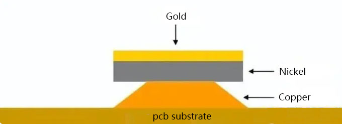
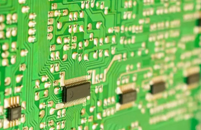
PCB surface finishing is the intermetallic connection between the bare copper in the solderable areas of printed circuit boards and the components. It usually refers to the outermost structure formed on top of the copper layer, which protects the copper layer and enhances solderability—equivalent to a “coating” on the copper.
A circuit board has a base copper surface. Without a protective coating, the base copper surface is easily oxidized, and the resulting copper oxide layer will significantly reduce soldering quality, thereby affecting the reliability and effectiveness of the final product. To prevent this problem, the PCB needs surface finishing.
PCB surface finishing is the most important step in PCB manufacturing, including fabrication and assembly. It has two main functions: one is to protect the exposed copper circuits, and the other is to provide a solderable surface for components during soldering to the PCB. As shown in the figure below, the surface finish is located at the outermost layer of the PCB, above the copper layer, acting as a “coating” on the copper.
Dual mission:
- Isolate oxygen/sulfides to protect the copper layer from oxidation
- Create an active surface to ensure the reliability of component soldering
Consequences of failure:
Experimental data show that the oxide layer thickness of an unprotected copper surface can reach 500 Å within 72 hours, leading to a drop in solder joint yield of more than 40%.
I. What is PCB Surface Finish?
PCB surface finish refers to the process by which, on the component contact areas and electrical connection points of a printed circuit board (PCB), a surface layer is artificially formed that differs from the base material in mechanical, physical, and chemical properties. This surface treatment not only protects the exposed copper surface from environmental factors such as oxidation but also provides a surface suitable for soldering, ensuring that components can be reliably connected to the PCB.
In addition, it must meet a series of functional standards, including but not limited to environmental protection requirements, electrical performance, physical strength, and durability, to ensure the high quality and long-term stability of the final product.
II. Technological Evolution: A History of Environmental Reform
PCB surface finishing technology has continually evolved with advances in electronic manufacturing processes and has mainly gone through the following stages:
- Initially, flux was applied directly to the copper surface for soldering. This process was simple but could not protect the copper surface for long, and soldering quality was greatly affected by the environment.
- When electronic products entered mass production, electroplated tin–lead (Sn–Pb) processes were widely adopted, which not only provided good solderability but also effectively protected the copper layer.
- With the introduction of solder mask technology, Hot Air Solder Leveling (HASL) became the mainstream process. By coating a layer of solder on the copper surface and leveling it with hot air, it improved soldering performance and reliability.
- As circuit board routing density increased, the requirements for surface flatness also rose, leading to the emergence of Organic Solderability Preservatives (OSP), which are environmentally friendly, low-cost, and suitable for the assembly needs of fine-pitch components.
- To meet the needs of clean assembly processes and long-term storage, Electroless Nickel/Immersion Gold (ENIG) began to be widely used and became favored for its excellent flatness and anti-oxidation capability.
- Subsequently, driven by increasingly stringent environmental regulations, lead-free processing became a trend, spurring the emergence of more new lead-free surface finishing technologies, such as:
- - Immersion Silver
- - Immersion Tin
- - Electroless Nickel Electroless Palladium Immersion Gold (ENEPIG)
- - Electroless Nickel Immersion Silver (ENIAg)
These new technologies not only provide good soldering performance but also take environmental protection into account, offering strong support for the manufacturing of high-density, high-performance electronic products.?
The EU RoHS Directive (2003) served as a watershed, driving three major technological innovations:
- Lead-free processing: SAC alloys replaced tin–lead.
- Flatness improvement: OSP/ENIG addressed fine-pitch soldering.
- Multilayering: the four-layer ENEPIG structure prevents “black pad.”
III. Comparison of Metal-Type Surface Finishing Options
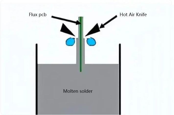
1. Hot Air Solder Leveling (HASL)
Hot Air Solder Leveling (HASL), also known as tin spraying, immerses the PCB in molten solder to form a solder layer on the copper surface; high-temperature compressed air (air knives) then blows off excess solder before it solidifies, making the surface flat and uniform. During the process, Cu–Sn intermetallic compounds (IMC) are formed, enhancing adhesion and soldering performance; the air knives reduce the meniscus effect and suppress bridging, improving soldering quality.
1.1 Leaded HASL
Alloy: Sn–Pb (typical 63/37, eutectic), with good wettability and solderability;
Low eutectic temperature of ~183 °C, wide process window, bright solder joints with high strength;
However, the lead content does not meet RoHS and other environmental requirements and is being gradually phased out.
1.2 Lead-Free HASL
Alloy: SAC (Sn–Ag–Cu), eutectic temperature ~217 °C; typical reflow 247–267 °C;
Solder joints are stronger and more environmentally friendly; the essential process is the same as leaded, only the alloy differs; it complies with the lead-free trend and is the mainstream choice.
Leaded vs. Lead-Free HASL: Comparison Table
> Recommend reading: HASL vs Lead-free HASL - PCB Surface Finishes
|
Dimension
|
Leaded HASL (Sn–Pb)
|
Lead-Free HASL (SAC)
|
|
Melting point / Reflow
|
Low (~183 °C)
|
High (~217 °C; reflow 247–267 °C)
|
|
Solder joint appearance
|
Bright, excellent wettability
|
Higher mechanical strength, environmentally friendly
|
|
Environmental compliance
|
Not RoHS-compliant
|
RoHS-compliant
|
|
Process fundamentals
|
Identical
|
Identical
|
|
Market trend
|
Being phased out
|
Mainstream
|
Process Essentials (including limitations)
● The PCB must be immersed in molten solder; excess solder is blown off with air knives before solidification;
● Air knives reduce the meniscus and prevent bridging;
● Limitations: surface roughness is relatively high, there are constraints for SMT; not suitable for contacts/tact switches; copper may dissolve when the board is subjected to high temperatures; manufacturing of thick/thin boards is restricted, making production inconvenient.
2. Immersion Tin (ImSn)
Immersion Tin (ImSn) is a metal-type surface finish in which a pure tin layer is deposited directly on the copper surface by a chemical displacement reaction. Since almost all solder systems are tin-based, ImSn is compatible with any solder. By adding organic additives to the tin bath, the coating can be made granular, thereby suppressing tin whiskers/tin migration and improving thermal stability and solderability. ImSn forms a flat Cu–Sn intermetallic compound (IMC) with copper, providing excellent flatness and solderability, and is suitable for SMT, fine pitch, and BGA.
Process Essentials
- Deposit pure tin on copper via chemical displacement; form a flat Cu–Sn IMC with stable solderability.
- High flatness; friendly to fine-pitch/BGA/small devices; suitable for horizontal production lines and fine geometries.
- Can maintain good solderability after multiple thermal excursions, but is sensitive to handling.
- Has certain erosion of the solder mask; not recommended to use together with peelable solder mask.
- Electrical test requires soft-probe solutions; not recommended for contact/tact switches.
- Shorter shelf life (tin-whisker risk after about 6 months); storage and turnover require attention.
Pros and Cons (table)
|
Item
|
Advantages
|
Disadvantages
|
|
Immersion Tin (ImSn)
|
Excellent flatness (suitable for SMT/fine pitch/BGA/small components); medium cost, lead-free; lamination-compatible; solderability maintained after multiple thermal excursions; suitable for horizontal lines and fine geometries
|
Sensitive to handling; short shelf life (≈ 6 months, tin-whisker risk); erosive to solder mask; not to be used with peelable solder mask; not suitable for contact switches; electrical test requires soft probes
|
Applicable / Limitations
- Applicable: fine-pitch SMT, BGA, smaller components, lead-free assembly, scenarios requiring good flatness.
- Limitations: long-cycle storage; contact parts/buttons; production lines with high requirements for electrical-test fixtures.
3. Immersion Gold — the appearance layer of the “Electroless Nickel/Immersion Gold (ENIG)” stack
“Immersion Gold” commonly appears as the appearance layer of Electroless Nickel/Immersion Gold (ENIG): first deposit a nickel (Ni) layer on the copper surface as a barrier/conductive layer, then deposit a thin gold (Au) layer for anti-oxidation and solderability. This system allows long-term storage and supports multiple reflows, with high surface flatness, suitable for high-density/fine-pitch assembly such as keypads and COB.
Process Essentials
- Typical structure: Cu/Ni/Au; during soldering, the gold layer quickly dissolves into the solder, and the IMC is mainly formed by the nickel layer.
- Flat, anti-oxidation, suitable for lead-free reflow and long-term storage.
- Pay attention to defect risks such as Black Pad (related to control of the electroless nickel chemical process).
- Cost is relatively high; aging/oxidation of the nickel layer may affect long-term reliability; solder joint strength is relatively weaker than tin-based coatings.
Pros and Cons (table)
|
Item
|
Advantages
|
Disadvantages
|
|
Immersion Gold (ENIG appearance layer)
|
Flat surface; suitable for high density/fine pitch; long-term storage and multiple reflows; suitable for keypads/COB
|
Higher cost; the nickel layer may oxidize over time; relatively weaker soldering strength; risk of Black Pad (requires strict process control)
|
Applicable / Limitations
- Applicable: high-density assembly, fine pitch, products requiring multiple reflows/long-term storage.
- Limitations: cost-sensitive situations; occasions with special requirements for very high solder joint strength.
4. Immersion Silver (ImAg, IMS, Immersion Silver)
Immersion silver sits between OSP and ENIG. It is easy to operate and fast, and it can still maintain good electrical performance and solderability under thermal/humid/contaminated environments (although the appearance will lose its luster). After cleaning/micro-etching the copper surface, a silver layer is deposited by a galvanic displacement reaction. Without a nickel underlayer, its physical strength is inferior to ENIG and it is more sensitive to creep corrosion (Creep Corrosion).
Process Essentials
- The displacement reaction directly deposits pure silver; rinsing/drying must be thorough to remove impurities.
- Multiple immersion-silver cycles or a silver layer >0.5 μm may corrode the copper layer due to the galvanic effect and lead to open-circuit risk.
- Easily reacts with environmental sulfides; can be stacked with OSP to suppress discoloration/sulfidation.
- Common applications: membrane switches, EMI shielding, aluminum wire bonding, very fine conductors.
- Short assembly window (must be assembled as soon as possible after opening); electrical testing is difficult.
Pros and Cons (table)
|
Item
|
Advantages
|
Disadvantages
|
|
Immersion Silver (IMS)
|
High solderability; flat surface; low cost, lead-free; suitable for aluminum wire bonding
|
High storage requirements, easily contaminated; short assembly window after opening; electrical testing is difficult; weaker resistance to creep corrosion; excessive thickness or repeated deposition has corrosion/open-circuit risks
|
Applicable / Limitations
- Applicable: high flatness requirements, aluminum wire bonding, EMI shielding, fine lines/membrane switches, etc.
- Limitations: high-sulfur/high-contamination environments, long storage cycles, production lines requiring convenient electrical testing.
5. Immersion Tin (IMT, Immersion Tin)
Immersion Tin (IMT) is an environmentally friendly chemical deposition process used to deposit a tin layer on the copper surface. It is commonly used in SMT and packaging applications and is intended to replace traditional Pb–Sn alloy electroplating. Tin is an amphoteric metal; after deposition, contact with strong acids/strong alkalis should be avoided. IMT improves product environmental friendliness and compatibility, meeting the needs of modern lead-free manufacturing.
Process Essentials
- Chemically deposit a tin layer that forms a Cu–Sn IMC with copper, with good flatness;
- Pay attention to chemical cleaning and surface activation, and avoid strong acids/strong alkalis;
- Similar to OSP, storage and assembly cadence need to be controlled to prevent surface aging and contamination.
Pros and Cons (table)
|
Item
|
Advantages
|
Disadvantages
|
|
Immersion Tin (IMT)
|
Environmentally friendly, lead-free; good flatness, suitable for SMT/packaging; compatible with solders
|
Sensitive to chemical environments (amphoteric); strict requirements for storage/turnover; long-term reliability and convenience of electrical testing are inferior to ENIG/ENEPIG
|
Applicable / Limitations
- Applicable: mass-production scenarios that pursue environmental protection, SMT flatness, and efficient chemical processing.
- Limitations: environments with exposure to strong acids/strong alkalis, long-term storage.
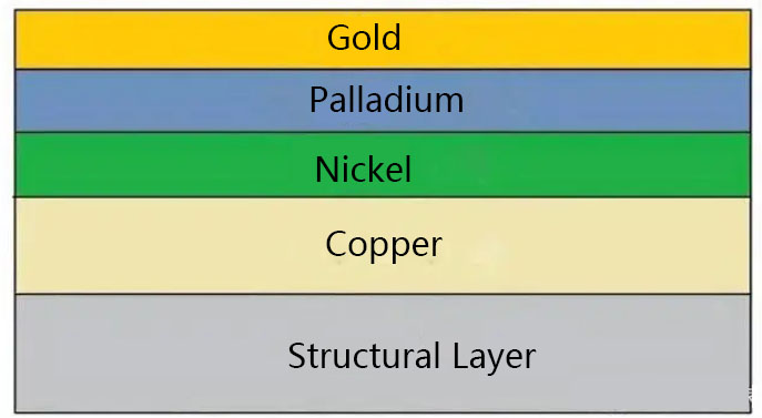
6. Electroless Nickel/Immersion Gold (ENIG)
ENIG (Electroless Nickel Immersion Gold) has a Cu/Ni/Au three-layer structure: electroless nickel (typically 3–5 μm) is deposited on copper as a barrier and soldering layer, and an immersion gold layer (~0.05–0.15 μm) is deposited on top as an anti-oxidation and solderable layer. During reflow, the gold layer dissolves into the solder at an early stage; the nickel is what actually forms the IMC of the solder joint. ENIG offers high flatness and a long shelf life, and is suitable for PTH and multiple reflow cycles.
Process Essentials
- Flow: cleaning → etching → activation → electroless nickel → immersion gold → cleaning of residues.
- If the Au content entering the solder joint >3%, the joint becomes brittle; the gold layer is recommended to be ≤0.3 μm.
- The process is complex and costly, and is usually not reworkable; RF circuits may exhibit signal loss.
- Strict control is required for failure modes such as black pad/black nickel.
Pros and Cons (table)
|
Item
|
Advantages
|
Disadvantages
|
|
ENIG
|
Flat surface; lead-free; suitable for PTH; long shelf life; suitable for multiple reflows and clean assembly
|
Expensive, not reworkable; risk of black pad/black nickel; possible RF signal loss; complex process
|
Applicable / Limitations
- Applicable: high density/fine pitch, PTH, products requiring long-term storage/multiple reflows, and products with requirements for assembly cleanliness.
- Limitations: cost/rework-sensitive cases; ultra-high-frequency, low-loss scenarios (RF evaluation required).
7. Electroless Nickel Electroless Palladium Immersion Gold (ENEPIG)
ENEPIG (Electroless Nickel Electroless Palladium Immersion Gold) has a Cu/Ni/Pd/Au four-layer structure. The palladium layer (0.1–0.5 μm) lies between nickel and gold; it protects the nickel layer from displacement corrosion during immersion gold, provides an excellent base for the gold layer, and significantly reduces the risk of black pad. The nickel layer is 3–6 μm, and the gold layer is 0.02–0.1 μm. ENEPIG offers excellent flatness/solderability/compatibility and is commonly used in high-end package substrates, multi-cycle assembly, and wire bonding.
Process Essentials
- Use the palladium layer to suppress key ENIG failures (such as black pad) and improve long-term reliability;
- The gold layer is very thin and soft; deep scratches may expose the palladium layer—mechanical protection is required;
- Can be used for wire bonding and multiple reflows; shelf life ≥12 months (under good control).
Pros and Cons (table)
|
Item
|
Advantages
|
Disadvantages
|
|
ENEPIG
|
Extremely flat; lead-free; multi-cycle assembly; excellent solder joints; wire bonding; essentially no black pad risk; long shelf life (≈12 months or longer)
|
Higher cost; reworkable but limited; high requirements for handling and thickness-uniformity control
|
Applicable / Limitations
- Applicable: high-end packaging, SiP, wire bonding, products with extremely high requirements for long-term reliability and flatness.
- Limitations: mass production with strict cost constraints.
8. Electroplated Nickel/Gold (Electroplated Ni/Au)
Electroplated nickel/gold sequentially deposits a nickel layer and then a gold layer on copper by electrochemical methods, used to suppress Cu–Au diffusion and to provide conductivity/wear resistance. According to the nature of the gold layer, it is divided into:
- Soft Gold (99.9%): used for wire bonding / high solderability;
- Hard Gold (99.6%): a gold alloy (containing cobalt/nickel/iron complexes), used for high-wear scenarios such as plug-in/contacts/gold fingers.
Typically, a 3–5 μm nickel layer is plated first, followed by 0.5–1.5 μm gold (depending on the application).
Process Essentials
- Adjust thickness and hardness via current density / time / solution composition;
- Soft gold has excellent solderability and bonding strength; hard gold is wear-resistant but not suitable for wire bonding;
- The real soldering IMC is still formed by the nickel layer, and the gold layer dissolves rapidly at the initial stage of soldering.
- Expensive; requires bus bars/segmentation, additional masking and etch-resist/tape steps; imposes higher requirements on layout/process.
8.1 Hard Gold
Hard electrolytic gold over low-stress nickel provides excellent wear resistance, making it suitable for edge-connector fingers, interconnect substrates, keyboard contacts, and other high-wear areas.
Process Essentials
- Military: gold 50–100 μin (>100 μin Ni base);
- Consumer: gold 25–50 μin;
- IPC solderable thickness recommendation: ≤17.8 μin (thicker reduces solderability).
- ~17 μin is generally not solderable; not suitable for wire bonding.
Pros and Cons (table)
|
Item
|
Advantages
|
Disadvantages
|
|
Hard Gold
|
Hard and wear-resistant; lead-free; long shelf life
|
Very expensive; many steps (electroplating/bus bars/segmentation/masking); difficult for other finishes to form; etch undercut or cause cracking/peeling; >17 μin not solderable; sidewalls outside gold fingers not fully encapsulated
|
8.2 Soft Gold
Soft gold has high purity (99.9%); its soldering/bonding performance is better than hard gold. It is suitable for wire bonding and for applications with higher requirements on solder-joint strength.
Pros and Cons (table)
|
Item
|
Advantages
|
Disadvantages
|
|
Soft Gold
|
Strong solderability/bondability; stronger solder joints
|
High cost; wear resistance is inferior to hard gold; also requires complex electroplating and masking processes
|
Applicable / Limitations
- Applicable: gold fingers / plug-in contacts (hard gold), wire bonding / solderability-first (soft gold), highly reliable electrical contacts (e.g., CPU sockets, memory modules).
- Limitations: strict cost constraints; non-contact areas that require full sidewall encapsulation.
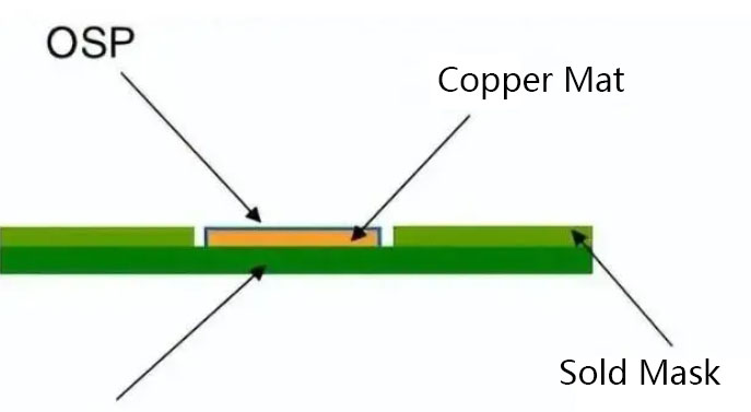
IV. Organic-Type Surface Finishing — OSP (Organic Solderability Preservatives)
OSP (also known as copper protector, Preflux) is a water-based organic molecule that selectively bonds with copper to form an organometallic layer (thickness about 0.10–0.60 μm), providing anti-oxidation/anti-sulfidation at room temperature; during reflow it is quickly removed by flux, and the bare copper immediately combines with solder to form a strong solder joint. Its function is limited to short-term solderability protection, but it is environmentally friendly, low-cost, and flat, making it very suitable for fine-pitch SMT.
Process Essentials
- Typical process: degreasing → micro-etching → acid wash → pure-water rinse → organic coating → rinse;
- Thickness cannot be measured (difficult to confirm online); an excessively thick coating may affect soldering;
- Not suitable for PTH; ICT may be affected; there is a risk of copper surface exposure before final assembly;
- Limited number of reworks (≤2 times); sensitive to handling;
- Not suitable for wave soldering/selective wave soldering (the surface is easily oxidized, causing soldering defects).
Pros and Cons (table)
|
Item
|
Advantages
|
Disadvantages
|
|
OSP
|
Flat, simple process, environmentally friendly, low cost; supports lead-free and SMT; reworkable; suitable for horizontal lines
|
Thickness cannot be measured; not suitable for PTH; short shelf life; may cause ICT issues; copper surface may be exposed during assembly; sensitive handling; limited rework times; not suitable for press-fit/wire insertion; inconvenient for visual/electrical test
|
Applicable/Limitations
- Applicable: cost-sensitive products, fine-pitch SMT, products with high flatness requirements but fast assembly cadence.
- Limitations: long-term storage, wave soldering/selective wave soldering, scenarios requiring PTH/ICT friendliness.
V. PCB Hybrid Surface Finishing Technology
A single surface finish is hard to cover all functional/cost/environmental needs, so hybrid surface finishing—using two or more processes in different areas on the same PCB—has become increasingly common, enabling a balance of high reliability in critical zones and cost reduction in non-critical zones.
Common Combinations
- ENIG + OSP
- Electroplated Ni/Au + ENIG
- Electroplated Ni/Au + HASL
- ENIG + HASL
- Lead-free HASL + gold fingers (electroplated hard gold)
Process Essentials
- Use immersion gold/electroplated gold in key connection/contact areas to ensure contact reliability, and use HASL/OSP in other areas to control costs;
- The sequence/masking/chemical compatibility of hybrid processes must be carefully designed;
- OSP uses water-based organic compounds that selectively bond with copper, which is more environmentally friendly than some metal finishes (the latter may have higher toxicity or energy consumption).
Applicable/Limitations (key-points)
|
Option
|
Applicable
|
Limitations/Notes
|
|
ENIG + OSP
|
High flatness/long-term reliability for critical pads + cost reduction in non-critical areas
|
Complex process sequence, high requirements for regional masking
|
|
Electroplated Ni/Au + ENIG
|
Balances contact wear resistance and soldering flatness
|
Complex electroplating fixtures/bus bars/masking, high cost
|
|
Electroplated Ni/Au + HASL
|
Wear resistance in contact areas + low cost in non-critical areas
|
Differences in surface height/solder accumulation need evaluation
|
|
ENIG + HASL
|
Flatness in fine-pitch areas + economy in conventional areas
|
Comprehensive failures such as RF/black pad/thermal shock need verification
|
|
Lead-free HASL + gold fingers
|
Wear resistance for plug-in contacts + economy for the rest
|
Hard-gold thickness and boundary control required in the gold-finger area
|
VI. How to choose PCB Surface Finish?
PCB finish selection is the most important step in PCB manufacturing because it directly affects process yields, amount of rework, field failure rates, testability, scrap rates, and cost. To ensure high quality and performance of the final product, all important considerations for assembly must be taken into account in the surface finish selection.
1. PCB Surface Finish - Pad Flatness
As mentioned earlier, certain surface finishes can result in uneven surfaces, which can affect performance, solderability and other factors. If flatness is an important factor, consider surface finishes with thin, uniform layers. In this case, suitable options include ENIG, ENEPIG, and OSP.
2. Solderability and Wettability
Solderability is always a key factor when working with PCBs, and specific finishes such as OSP and ENEPIG have been shown to hinder solderability, while other finishes such as HASL are well suited.
3. Gold or Aluminum Wire Bonding
If your PCB requires gold or aluminum wire bonding, it may be limited to ENIG and ENEPIG.
4. Storage Conditions
As mentioned earlier, some finishes (such as OSP) can make PCBs brittle when handled, while other finishes increase durability. Prior consideration should be given when considering storage and handling requirements, and surface treatments that make PCBs brittle should be used only when risk-free storage and handling requirements can be met.
5. Soldering cycle time
How many times does a PCB have to be soldered and reworked? Many finishes are ideal for rework. However, other methods such as immersion tin are not suitable for rework.
6. PCB Surface Finish - RoHS Compliance
RoHS compliance is critical when determining the surface finish to be used. Generally, all finishes that use lead are not RoHS compliant and should be avoided.
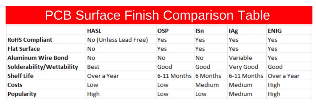
Based on the description of each surface finish above, a number of attributes are the most important elements to use as selection criteria. The table below shows the attributes that each surface finish does and does not have.
Depending on the specific requirements and characteristics of the PCB product, you can follow this table to select the perfect surface finish option.
Conclusion
When choosing PCB surface finishing, the process's fitness for purpose is always more important than fame: your component pitch, assembly process (reflow/wave/selective soldering), long-term storage needs, contact wear resistance, RF loss tolerance, and cost targets will all directly affect the final decision. To this end, NextPCB provides comprehensive finish selection and manufacturing collaboration, allowing design–manufacturing–assembly to start within the same process window from the very beginning.
NextPCB's comprehensive capabilities in surface finishing and manufacturing
Full spectrum of surface finishes: HASL (leaded/lead-free), ImSn (immersion tin), ImAg (immersion silver), ENIG (electroless nickel/immersion gold), ENEPIG (electroless nickel electroless palladium immersion gold), electroplated Ni/Au (hard gold/soft gold), OSP, and selective/partitioned hybrid finishes (such as “gold finger electroplating + other areas ENIG/HASL/OSP”).
- Manufacturing and assembly collaboration: supports multilayer/HDI, impedance control, high TG, thick copper, blind/buried vias/microvias, gold-finger chamfering, countersunk holes, V-Cut, selective electroplating, etc.; also provides one-stop SMT/PCBA (including BOM compatible alternatives, process fixtures, functional testing/aging, traceable barcodes).
- Quality control and data-based verification: XRF coating-thickness measurement, microsection (cross-section) analysis, ion contamination (ROSE) and solderability testing, 100% electrical test and AOI; materials and test reports (such as RoHS/physical properties/thickness data) can be provided as needed to support audits and compliant delivery.
- Engineering support (DFM/DFX): for fine-pitch/BGA/RF/high-speed/automotive/medical scenarios, provide surface-finish selection recommendations, reflow curves and assembly-window collaboration, impedance/material stack-up recommendations, reducing rework and failure rates in the early design stage.
- Delivery and service: smooth capacity expansion from prototyping to small batch to mass production; expedited options and global logistics support; one-to-one process-engineer communication to shorten the time to close issues.
How to get started quickly with NextPCB
- Still hesitating about which surface finish to choose? Send us your minimum component pitch, whether there are gold fingers/plug-in contacts, the assembly process (reflow/wave/selective soldering), whether long-term storage is required, and whether there are RF/high-speed lines. We will provide two to three feasible process routes (including pros/cons and notes) based on cost and reliability.
- Already have files ready to place an order? Directly upload Gerber/ODB++, BOM, and coordinates (Pick & Place), and note “surface-finish priority and alternatives.” If hybrid finishes or selective electroplating are required, mark the areas and boundaries. Engineers will conduct DFM review and confirm thickness/flatness/solderability windows.
- Want price comparison or risk assessment? Provide the current plan and pain points (such as black-pad risk, tin-whisker concerns, ICT yield, contact wear, RF insertion loss, storage-period requirements). We can issue targeted improvement suggestions and process comparison lists.
Act now: send us your project key points or documents, and let NextPCB's engineering team use the right surface finish + the right manufacturing window to help you get yield, reliability, and cost all right at the same time.
About the Author
Julia Wu - Senior Sales Engineer at NextPCB.com
With over 10 years of experience in the PCB industry, Julia has developed a strong technical and sales expertise. As a technical sales professional, she specializes in understanding customer needs and delivering tailored PCB solutions that drive efficiency and innovation. Julia works closely with both engineering teams and clients to ensure high-quality product development and seamless communication, helping businesses navigate the complexities of PCB design and manufacturing. Julia is dedicated to offering exceptional service and building lasting relationships in the electronics sector, ensuring that each project exceeds customer expectations.


 NextPCB Capabilities
 PCB Assembly
 Layer Buildup
 SMD-Stencils
 PCB Design-Aid & Layout
 Mechanics
 Surface
 Quality
 Drills & Throughplating
 Factory & Certificate


