
 Surface


Julia Wu - Senior Sales Engineer at NextPCB.com

 NextPCB Capabilities
Printed Circuit Boards
NextPCB Capabilities
Printed Circuit Boards
 PCB Assembly
 Layer Buildup
 SMD-Stencils
 PCB Design-Aid & Layout
 Mechanics
 Quality
 Drills & Throughplating
 Factory & Certificate
 PCB Assembly Factory Show
Certificate
PCB Assembly Factory Show
Certificate
Support Team
Feedback:
support@nextpcb.com


In the last two decades, flying probe test has gained popularity when it comes to ensuring that circuit boards are manufactured right. As demand has grown, more and more people are using FPTs.
PCBs use several components, like integrated circuits (ICs), resistors, capacitors, transformers, inductors and transmission lines. These parts are all mounted so that the board will work as designed. To make sure all the individual components are mounted correctly and still work together efficiently in the package, there is testing and inspection. Some important tests for your PCB include PCB flying probe test, bed of nails test, and in-circuit test. Out of these methods, PCB flying probe is one worthwhile method which has evolved through various stages of automation and compatibility requirements. The PCB assembly house should have an adequate understanding of this highly efficient PCB testing technique before adopting it - that's why this post provides detailed information about the integrated circuit (IC) pins site inspection testing procedure or flipping method; its significance, features and applications.
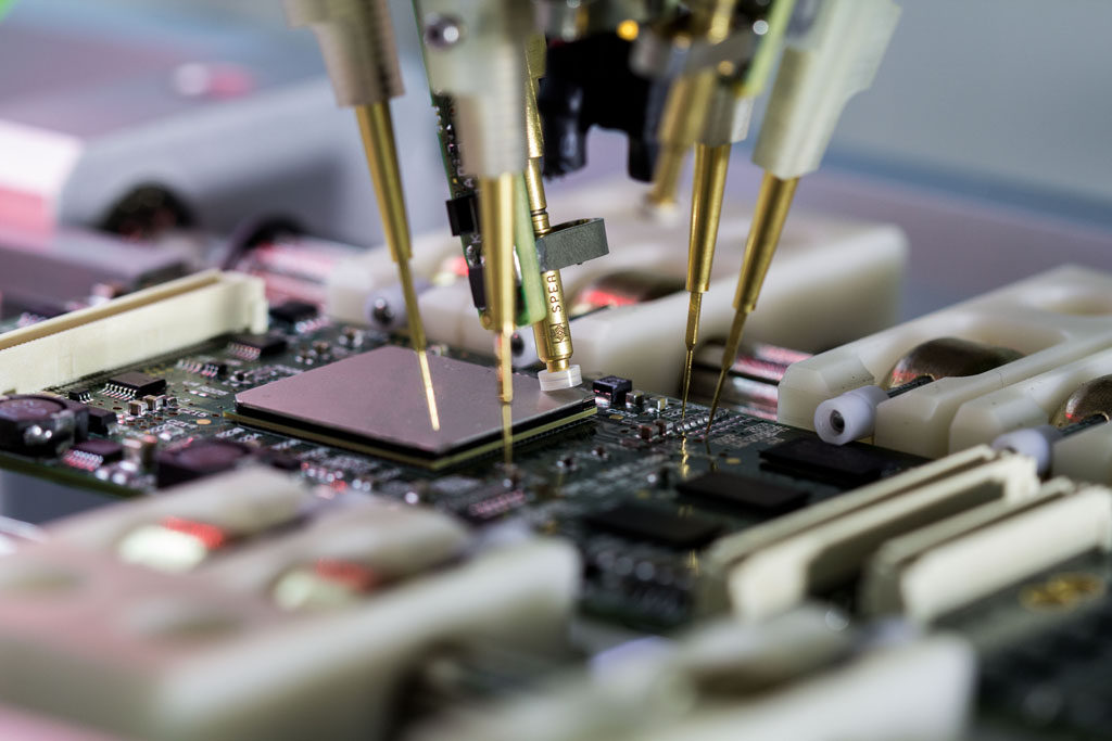
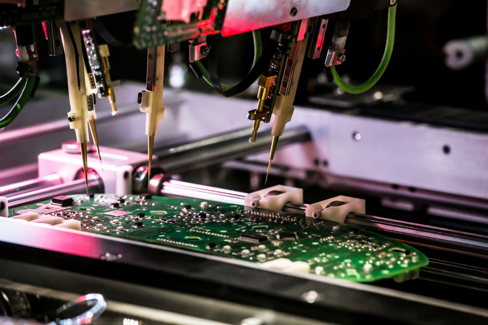
Flying probe testing is an in-circuit test method used in the electronics industry to test printed circuit board assembly. It is a test method that utilizes multiple probes to make electrical contact with the test points of a PCB assembly. The probes are "flown" over the surface of the board, making contact with the test points. The test results are then analyzed to determine if the board meets the expected requirements. Flying probe testing is a cost-effective way to test PCBs and is commonly used in high-volume production.
Flying probe testing is a quicker and more cost-effective method of testing when there are only a few circuits to test. It can also be used to test prototypes before the board goes into full production.
The main advantage of the test is that it can be completed quickly and made available to many individuals; this makes it a great option when you need to get your product on the market in a matter of days or hours. Coverage is also at a high level, meaning the test can focus on specific features or faults within your design.
Here's how flying probe testing work:
1. The first step in the flying probe testing process is to create the test program. This program will contain the instructions for the probes to test the board, such as the type of tests to be performed, the voltage levels to be used, and the locations of the test points on the board.
2. Once the test program has been created, the test probes are then moved into position. The probes are mounted on a platform that can be moved along the X, Y and Z axes in order to position the probes over the test points on the board.
3. Once the probes are in position, the test program is then executed. The probes will make contact with the test points on the board, and apply the required voltage levels. The test program will then measure the electrical parameters of the test points, such as current, resistance, capacitance, and inductance.
4. Once the test is completed, the results are then analyzed to determine if the board is functioning properly. If any errors are detected, then the board may need to be reworked or replaced.
Flying probe testing is an efficient and cost-effective method of testing PCBs. It can be used to identify and fix problems before the boards are sent out for assembly, which can save time and money. Additionally, flying probe testing is a non-invasive technique, which means that the board does not need to be taken apart in order to be tested. This makes the process faster and more efficient.
@nextpcbofficial #pcb #factory #components #smt #maker #teaching #fyp #electronic #nextpcb ♬ original sound - NextPCB
The advantages of using a flying probe test are numerous. First, it is a cost-effective way to test circuits and boards. Because the probes are able to move freely, they can reach many points of a board without needing to be repositioned. This reduces the amount of time and labor required for testing, resulting in a lower cost.
Second, the flying probe test is very accurate. The probes are able to measure the electrical characteristics of a board with a high degree of accuracy. This is important for ensuring that the board meets the specifications of the design.
Third, the flying probe test is fast. The probes can move quickly around the board, allowing the test to be completed in a short amount of time. This is beneficial when time is of the essence, such as when a product needs to be released to market quickly.
Fourth, the flying probe test is flexible. The probes can be programmed to move in various patterns, allowing them to test different types of circuits and boards. This makes it possible to test a variety of products with the same testing system.
Finally, the flying probe test is safe. The probes are protected by a guard, which prevents them from coming into contact with any other components or people. This helps to reduce the risk of any damage or injury that could be caused by faulty circuit boards.
Overall, the flying probe test is an efficient and cost-effective method for testing circuit boards. It is accurate, fast, flexible, and safe, making it the ideal solution for many types of testing requirements.
The flying probe test is a type of electrical test that is used to test printed circuit boards (PCBs). This type of testing is often used in the production of PCBs in order to test the functionality of the board before it is shipped out to customers. While flying probe testing offers many advantages, there are also some disadvantages that should be considered when deciding whether or not to use this type of testing.
One of the primary disadvantages of flying probe tests is its limited accuracy. This type of test is not as accurate as other testing methods, such as automated optical inspection (AOI). While a flying probe test can still provide some detailed insight into the functionality of a board, it cannot detect some faults that may be present. This is especially true for smaller, more complex boards.
Another disadvantage of flying probe tests is its relatively high cost. While the cost of this type of testing is not incredibly high, it is still more expensive than other methods, such as AOI. This makes it difficult to justify the cost of this type of testing for some companies.
The setup time for flying probe test is also a significant disadvantage. This type of testing requires the setup of test probes and other equipment, which can be time-consuming. This can be especially problematic when testing large numbers of boards in a short period of time.
The flying probe test is also limited in terms of its flexibility. This type of testing requires specialized equipment and is not as flexible as other methods. This can be problematic when testing boards with different designs or sizes, as the test probes may need to be adjusted for each board.
Finally, the flying probe test is limited by the number of test points that can be tested at one time. This can be problematic when testing large boards with many test points, as it may not be possible to test all of them in a single run. This can lead to longer test times and potentially missed faults.
Overall, flying probe test is a useful tool for testing PCBs, but it does have some significant drawbacks. It is important to consider these drawbacks when deciding whether or not to use this type of testing for a particular project.
The printed circuit board (PCB) industry uses several test methods to ensure that all boards are manufactured correctly and that any design flaws are identified and corrected. While most of these tests are done in the fabrication process, many of them can also be done in-house. The following are some of the most common PCB tests used in the industry.
In-Circuit Test (ICT): This is one of the most common tests used in the PCB industry. It involves testing each component on the board to check for proper functionality. In-circuit testing is often used to test for continuity, shorts, and opens, as well as other types of faults.
Functional Test: This test is used to check the functionality of the board. It involves testing the board's performance against a set of predetermined criteria. This is usually done by connecting the board to a test jig, and then running through a set of tests to check the board's performance.
Visual Inspection: This is the most basic test used in the PCB industry. It involves examining the board visually to check for any visible defects. This includes checking the board's solder joints, components, and other features to ensure they are in proper condition.
X-Ray Inspection: This is a more advanced test used to inspect the board internally. It involves using a specialized X-ray machine to take a picture of the board, which can then be used to check for any hidden defects or flaws.
Thermal Imaging: This test is used to check the board's temperature. It involves placing the board in a thermal chamber and then measuring its temperature at various points. This helps to identify any areas where there may be hot spots, which can indicate a problem with the board's design.
Electromagnetic Interference (EMI) Test: This test is used to check the board's ability to withstand electromagnetic interference. It involves running the board through a series of tests, which measure the board's ability to block out electromagnetic signals.
Solderability Test: This test is used to check the board's ability to accept solder. It involves running the board through a series of tests to check the board's solderability, which helps to identify any areas that may be prone to soldering defects.
Electrical Test: This test is used to check the board's electrical characteristics. It involves running the board through a series of tests to check its resistance, capacitance, and inductance.
These are some of the most common PCB test methods used in the industry. While most of these tests are done in the manufacturing process, many of them can also be done in-house. Performing these tests can help to ensure that all boards are manufactured correctly and that any design flaws are identified and corrected.
> Recommend reading: PCB Manufacturing Basics: Design, Fabrication, Testing, and Compliance
In conclusion, the flying probe test is one of the most efficient and cost-effective methods of testing PCBs. It is accurate, fast, flexible, and safe, making it the ideal solution for many types of testing requirements. Although there are some drawbacks to using this type of testing, such as limited accuracy and higher cost, it can still be a useful tool when testing large numbers of boards in a short period of time. Additionally, there are several other test methods that are used in the PCB industry, such as in-circuit tests, functional tests, visual inspections, X-ray inspections, thermal imaging, EMI test, solderability test, and electrical test. Using these tests, can help to ensure that all boards are manufactured correctly and that any design flaws are identified and corrected.

Still, need help? Contact Us: support@nextpcb.com
Need a PCB or PCBA quote? Quote now

