Contact Us
PCB Manufacturing & Assembly for Key Industries Contact Us
Standard PCB Capabilities

PCB Manufacturing & Assembly Services for Key Industries | NextPCB

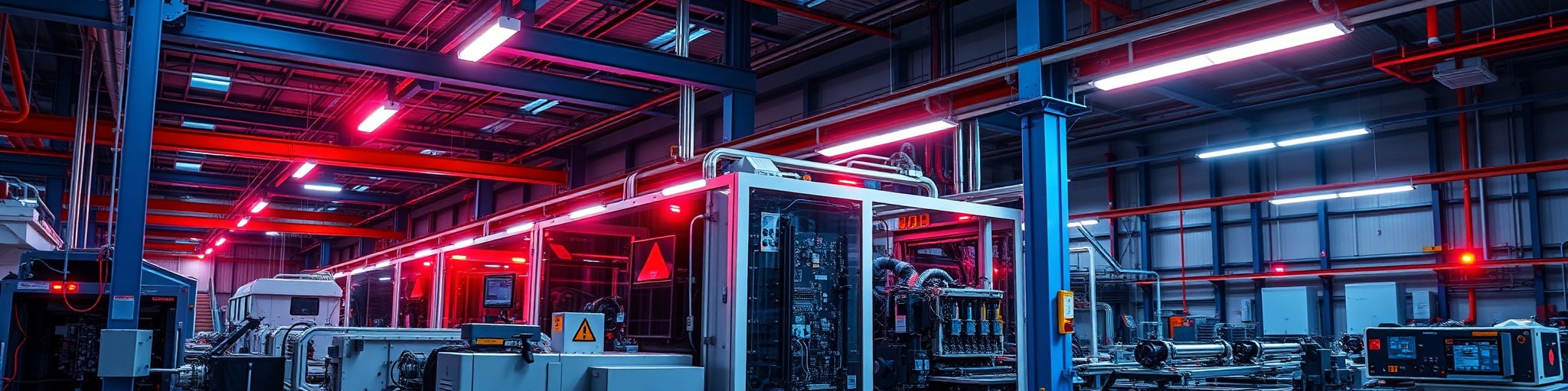
Providing Custom PCB Solutions Tailored to Meet the Demands of Various Industries

NextPCB Capabilities

Industry-Specific PCB Manufacturing & Assembly Solutions

NextPCB delivers mission-critical circuit board solutions tailored for demanding sectors. From ISO 13485 certified medical boards to high-frequency 5G telecommunication modules, our manufacturing capabilities meet the rigorous standards of reliability, precision, and performance required by your industry.

5G / RF

Communication

Optimized for high-speed signal integrity and low transmission loss.

  • Rogers & Taconic High-Frequency
  • Strict Impedance Control (±5%)
  • Signal Integrity via Back-drilling
PLC / Robotics

Industrial Automation

Built for durability in harsh, complex environments.

  • High-TG Materials for Stability
  • Multi-layer Boards (Up to 20)
  • Press-fit & Blind/Buried Via
HDI / SMART

Internet of Things (IoT)

Miniaturized PCB solutions for ultra-compact smart connectivity.

  • Any-layer HDI (1+N+1)
  • Minimum Trace/Space 3/3 mil
  • Rigid-Flex PCB for Wearables
PCBA / MASS

Consumer Electronics

Cost-effective mass production for innovative high-volume devices.

  • Turnkey PCBA (01005)
  • ENIG & OSP Quality Finishes
  • Quick-turn to High-Volume Scaling
STABILITY

Security & Surveillance

Reliable solutions for 24/7 monitoring and HD systems.

  • High-Precision LDI & AOI
  • Complex BGA Pitch Soldering
  • Certified Long-Lifecycle Control
ISO 13485

Medical Electronics

Precision-grade manufacturing for life-critical healthcare devices.

  • IPC Class 3 Standards
  • Component Sourcing Traceability
  • Comprehensive ICT & FCT Testing
HEAVY COPPER

Power Industry

Robust designs for high-voltage, high-current management.

  • Heavy Copper PCBs (Up to 12oz)
  • Aluminum Core & Metal-Base
  • Advanced Thermal Management
IATF 16949

Automotive

IATF-certified solutions for ADAS, EV systems, and ECU control.

  • IATF 16949 Certified Production
  • Ceramic PCBs & Thermal Substrates
  • Full PPAP Level 3 Documentation

Manufacturing Standards by Industry

Medical

ISO 13485:2016

Class 2/3 Capabilities

Automotive

IATF 16949

AEC-Q Compliant Components

Aerospace

ISO 9001:2015

Strict Tolerance Control

General

UL Certified (E-file)

RoHS & REACH Compliant

Frequently Asked Questions

Why do PCB projects often get delayed due to supply chain issues, and how can I avoid this?
In PCB manufacturing and assembly, delays often stem from component shortages and long lead times for critical parts (e.g., RF components, passives, microcontrollers). These supply chain challenges can slow down prototype delivery and mass production.

To reduce risk, it’s essential to prepare your Bill of Materials (BOM) early, include approved alternatives, and leverage component sourcing services. NextPCB provides integrated PCB manufacturing, parts sourcing & turnkey PCB assembly solutions, helping you secure components and shorten cycle time. Our engineering team can also recommend commonly available parts and compliant substitutes to prevent bottlenecks. Learn more about our component sourcing services.

>> We help streamline PCB supply by coordinating manufacturing, procurement, and assembly for various PCB types (including high‑frequency 5G, HDI, automotive & industrial PCBs). Discover our expertise in high-frequency 5G PCBs and other industry-specific solutions.
Why do PCB designs get rejected at the manufacturing stage, and how can I reduce rework?
PCB designs often get flagged due to issues uncovered during manufacturability review — things like incorrect footprints, too‑tight trace spacing, improper copper clearance, or layer stack‑up violations. These issues lead to manufacturability failures, rejected files, or production delays.

NextPCB encourages early Design for Manufacturability (DFM/DFA) checks before production. Utilizing our free Gerber viewer and DFM tools, designers can verify rules and adjust accordingly. By aligning your PCB layout with manufacturing capabilities and constraints, you can significantly reduce returns, improve yield, and accelerate your PCB’s path from prototype to volume manufacture. Try our DFM check tool.

>> We support DFM guidance for multilayer, HDI, rigid‑flex, and high‑speed boards, ensuring your design is ready for reliable fabrication and assembly. Learn more about our Advanced PCB Manufacturing Capabilities.
What are the most common PCB quality failures, and how does NextPCB ensure reliable boards?
Common PCB and PCBA quality issues include weak/inconsistent solder joints, misaligned parts, insufficient plating in vias, and errors in surface finish application. These problems can originate from design oversights, component mismatches, or inconsistent fabrication/assembly quality.

NextPCB mitigates these risks with a robust quality management process — multiple inspection stages including SPI, AOI, X‑ray, functional testing, and ICT/E‑Test — alongside international certifications (ISO9001, IATF16949, ISO13485, RoHS/REACH). This ensures every bare board and assembled PCB meets performance expectations. To learn more about our quality standards, browse NextPCB's quality certifications and test reports.

>> Through controlled manufacturing processes and thorough testing, we support reliable PCB production from prototypes to mass production. Check out our PCB assembly services for further details.
How can I ensure signal integrity and impedance control for high‑frequency, 5G, or RF PCB designs?
For high‑frequency or RF designs (like 5G modules and high‑speed communication boards), precise impedance control, stack‑up design, and material selection are essential to ensure signal integrity and reduce loss. Commonly used low‑loss substrates such as Rogers, Isola, or high‑TG materials help maintain performance.

NextPCB offers ±5% impedance control, stack‑up optimization, and advanced processing options tailored for high‑frequency, high‑speed, and RF PCBs. Designers should define key parameters (material dielectric constant, copper weight, trace width/spacing) early and consult with manufacturing engineers to optimize performance. Check our impedance control services.

>> Our support includes guidance on stack‑up configuration, impedance calculators, and compliance with industry standards to help you achieve consistent signal integrity. Learn more about our high-speed PCB solutions.
I’m a startup or small project developer — how can I lower PCB costs and get prototypes faster?
For innovators, startups, and low‑volume projects, cost and speed are major considerations. NextPCB provides quick‑turn PCB prototyping services (even 24‑hour options) and small batch PCB + turnkey assembly at competitive pricing, including standard finishes like ENIG and OSP.

To further reduce cost and accelerate delivery:
  • Use standard board materials and thicknesses
  • Choose common surface finishes
  • Provide complete BOM and pick‑and‑place data up front
  • Take advantage of our free DFM review and quote tools
>> With online instant quoting, panelization guidance, and procurement support, we make it easier to go from design files to assembled boards — even for small orders or rapid iterations. Learn more about our quick-turn PCB prototyping services.

Ready to start your project?

Get a free quote for your industry-specific PCB needs today.