Design Rule Check
Posted: 09:15 AM January 02, 2020
writer: NextPCB
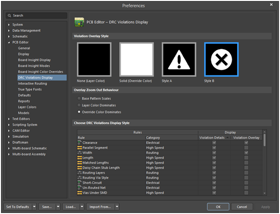
Design rule check, more commonly called as DRC in the PCB industry, is a physical design process to determine if the physical layout satisfies a number of rules or recommended parameters defined by the semiconductor manufacturers. DRC also involves LVS(layout and schematic)inspection, XOR inspection, ERC (electrical rule inspection), and antenna inspection.

What is the function of the design rule check (DRC)?
PCB design rules are the geometric constraints on designers of circuit boards, semiconductor devices, and integrated circuits (ICs) to ensure that their designs’ regular operation, reliability, and can be produced at acceptable yields. Since electronic design automation is widely used, DRC is a vital process to ensure designers maintain the minimum clearance rules and do not violate design rules. The main function of DRC is to achieve the reliability of the design and high overall yield. It is better to perform a batch mode design rule check before generating the final artwork. Besides, DRC is a necessary step to ensure the normal variability in the fabrication process conforms to the rules and does not result in chip failure.
Designers usually design the boards in their own PCB design software, but the Gerber file is needed to send to the PCB manufacturers to create a physical PCB. DRC will help designers to pay attention to the logical and physical constraints in the world of PCB manufacturing. Most of the PCB design software will provide the DRC function. Only the rules, such as trace widths, via diameters, and component spacing, have been set up in PCB design software, and then designers can go on the design process. DRC offers the designer a great convenience in PCB design because it is difficult to fix DRC errors after the PCB layout. Most software leaves the design rules at the default value, but designers may set up some custom rules in advance for more professional PCB projects.
Parts of the examples of DRC in PCB design
- DRC checks if the spacing constraints including the space between the trace, the trace and the via, the trace and the pad, the via and the pad, and the space between the vias are reasonable or not. And whether the space design suitable for production or not.
- Check the length of the traces and the guard wires and check whether the input and output lines are separated.
- Check the width of the power line and ground wire and check if the two are tightly connected.
- Check if there are short circuits or not, and Check whether the icons and labels added on the board can cause a short circuit.
- Check whether the resistance welding meets the production process requirements and whether the wielding size is appropriate.
The PCB production will be a game of luck if without the DRC. A comprehensive DRC can help designers to recognize many unwanted mistakes in advance and help both customers and manufacturers to minimize the damage and cost from failed circuit boards. If you have any problems with the PCB design when doing a PCB prototype, please contact us for further communication.
 PCB Assembly
 Layer Buildup
 Online Tools
 PCB Design-Aid & Layout
 Mechanics
 SMD-Stencils
 Quality
 Drills & Throughplating
 Factory & Certificate
 PCB Assembly Factory Show
Certificate


