
 Surface


Lolly Zheng- Sales Account Manager at NextPCB.com

 NextPCB Capabilities
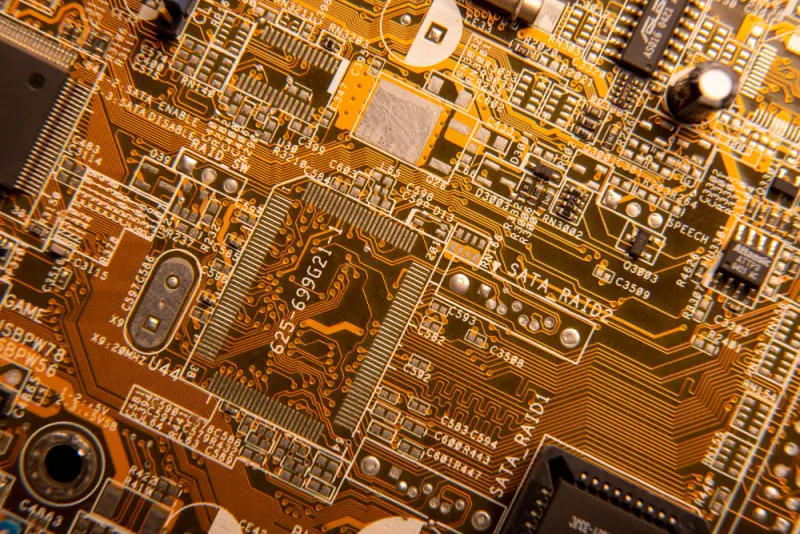
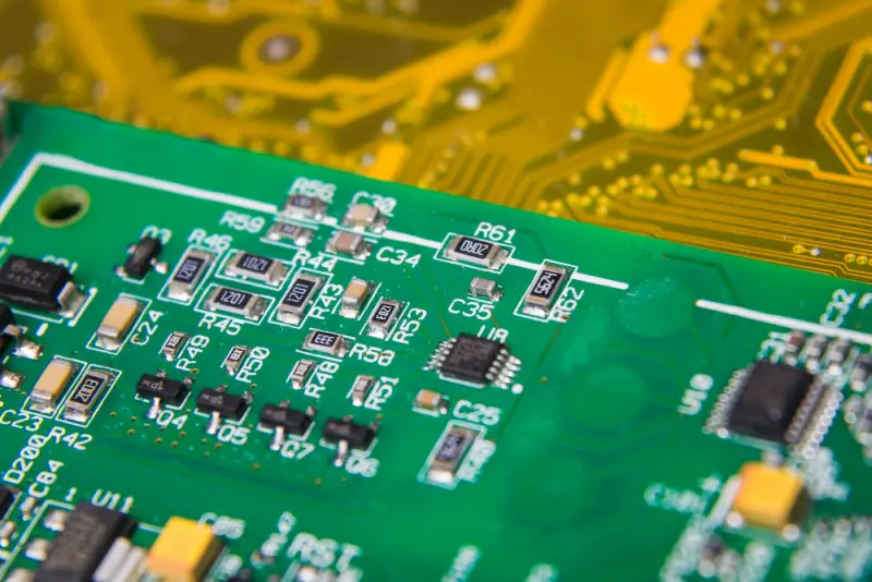
Printed Circuit Boards
NextPCB Capabilities
Printed Circuit Boards
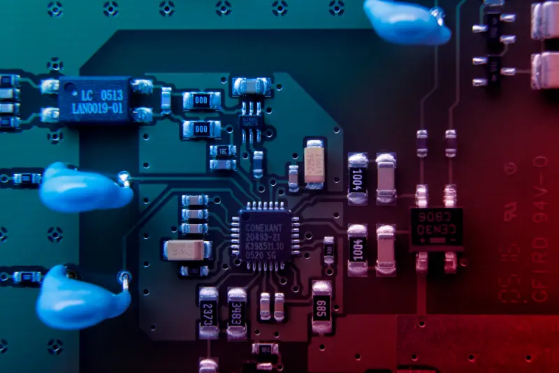
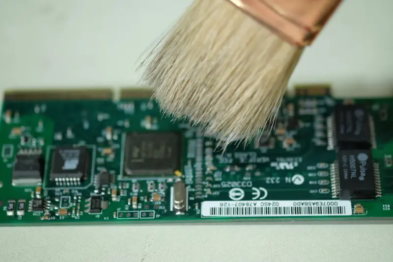
 PCB Assembly
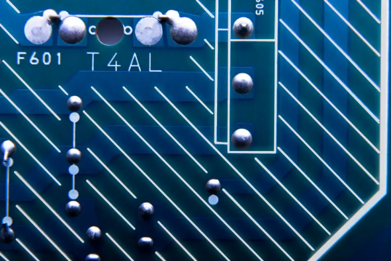
 Layer Buildup
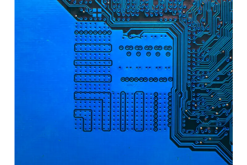
 SMD-Stencils
 PCB Design-Aid & Layout
 Mechanics
 Quality
 Drills & Throughplating
 Factory & Certificate
 PCB Assembly Factory Show
Certificate
PCB Assembly Factory Show
Certificate
Support Team
Feedback:
support@nextpcb.com


Introduction: The DFX Philosophy for Modern PCB Design
The success of a modern electronic product depends on a comprehensive, forward-thinking approach known as Design for Excellence (DFX). This holistic design philosophy goes beyond basic electronic connectivity, asking a critical question: "Can this PCB be manufactured with the highest possible yield, at the lowest feasible cost, and through a stable, repeatable process?"
This guide focuses on the three core pillars of DFX, each optimizing a specific stage of the production process:
These disciplines are deeply intertwined. The goal of an elite designer is to balance these requirements to achieve a truly production-ready design, updating and expanding on older "basic rules" with contemporary best practices.
> Get a Free DFM/DFA Review + Instant PCBA Quote at NextPCB (Free DFM/DFA review is supported in NextPCB’s turnkey PCBA flow.)

The journey of a PCB design begins with its physical form. Defining the board's size and shape early is a fundamental DFM practice, as these mechanical constraints are non-negotiable and dictate the entire layout. The PCB must fit within its final product's enclosure and accommodate all mounting holes, connectors, and other mechanical features. While rectangular boards are most common and cost-effective, designs may require irregular shapes to fit a specific product form factor. Crucially, designers must establish a buffer zone or edge clearance. This is a vital DFM consideration, as components and critical traces should be kept away from the board's perimeter to prevent damage during depanelization (separating the boards from a panel) or from mechanical stress during assembly. A recommended practice is to maintain a minimum distance, often cited as at least 10 mil (0.01 inches), between copper features and the board edge to ensure solder mask gaps and prevent encroachment on pads.
> Check NextPCB Manufacturing Capabilities & Design Rules

Choosing the right number of layers for a PCB is a direct trade-off between design complexity, performance, and cost. While a simple board may only need two layers, complex, high-speed designs may require four, six, or even more layers to manage routing density, signal integrity, and power delivery. A well-engineered stack-up is crucial for a product's performance, as it effectively addresses issues such as electromagnetic interference (EMI), signal crosstalk, and impedance mismatch.
> Recommend reading: What is EMI and EMC in PCB?
A proper stack-up balances electrical requirements with mechanical realities. An often-overlooked DFM consideration is the distribution of copper across the layers. A symmetrical stack-up structure, where layers are arranged in a balanced fashion from the center outwards, is a best practice. This design approach helps prevent board warpage, also known as bow and twist, which can be a direct result of non-uniform thermal expansion during the high-temperature reflow soldering process.
The underlying principle is that different materials (FR-4 core, prepreg, copper) expand and contract at different rates when heated. An unbalanced design can create significant mechanical stress, causing the board to deform. This warping, in turn, can lead to severe assembly issues. For instance, a warped board may not be able to form a proper seal with the solder paste stencil, leading to printing defects, or it can cause components, especially fine-pitch ones like BGAs, to lose contact with their pads, resulting in poor solder joints and costly rework. A symmetric layer arrangement and a balanced copper distribution are fundamental DFM strategies that directly improve assembly yield and product reliability by ensuring the board remains mechanically stable throughout the entire production process.
To maximize manufacturing efficiency and reduce per-board costs, multiple individual PCBs are often fabricated and assembled together on a single, larger panel. This process, known as panelization, streamlines handling, automation, and material usage. The method used to separate the boards from the panel is a critical DFA/DFM choice that affects cost, speed, and the stress on components.
There are two primary panelization methods: V-scoring and tab routing. V-scoring is a cost-effective and fast method ideal for high-volume production of simple, rectangular boards. It involves cutting V-shaped grooves into the top and bottom of the panel, weakening the material along the separation lines so that the boards can be snapped apart. However, this method is limited to straight lines and can put moderate stress on components near the edge, potentially leaving a rough finish. In contrast, tab routing uses a CNC router to cut the boards out, leaving small connecting tabs that are broken later. This method is more flexible, accommodating irregular shapes and curved outlines. It is also gentler on delicate components and can be customized to avoid sensitive areas. The primary trade-off is a higher cost and slower process due to the precise CNC machining and the need for manual cleanup of the tab remnants, often referred to as "mouse bites".
This comparison illustrates a clear design choice based on the project's needs. V-scoring offers a cost-effective, fast solution for simple designs and high-volume production, while tab routing provides the flexibility and gentleness required for complex shapes and delicate boards.
In the world of automated PCB assembly, precision is paramount. Automated pick-and-place machines and solder paste printers rely on visual cues to accurately position the board and place components. These cues come in two forms: fiducial marks and tooling holes.
Fiducial marks are small, circular copper pads with a solder mask opening that serve as optical reference points for machine vision systems. They are crucial for correcting alignment and orientation errors. There are two types: global fiducials, which are placed in the corners of a single PCB or a panel to align the entire board, and local fiducials, which are placed near fine-pitch components like BGAs to provide ultra-precise local alignment.
The recommended practice is to place at least three global fiducials on each board or panel. Placing them in a non-symmetrical, triangular pattern is a strategic choice that enables the machine's vision system to perform more than just simple X-Y and rotational corrections. During manufacturing, PCBs can experience minor stretching, shrinking, or twisting due to thermal stress. A three-point fiducial system allows the machine to measure the distances between the marks and compensate for these non-linear distortions on the fly, ensuring every subsequent component is placed with micro-level precision despite any subtle board deformation. This proactive correction is a fundamental aspect of high-yield automated assembly for high-density boards.
Tooling holes are non-plated mechanical holes that aid in precisely aligning and clamping the PCB to the assembly fixture. These are typically placed at opposing diagonal corners and provide a physical datum for the entire panel or board. Both fiducial marks and tooling holes are essential for streamlined, high-quality production, ensuring that the physical board aligns perfectly with the digital design files.
> Run a Free HQDFM Check on Your Gerbers Before Ordering
The efficiency and success of a PCB assembly are determined long before a single part is soldered. The way components are arranged, known as floor planning, is a critical DFA practice that directly impacts routing complexity, signal quality, and manufacturability. A top-down approach is highly recommended: start by placing connectors and critical components like microcontrollers, which often have fixed locations dictated by the product's enclosure.
From there, group related components into functional blocks, such as power supply, analog, or digital sections. This logical organization minimizes trace lengths, reduces signal interference, and simplifies the routing process. For example, decoupling capacitors should be placed as close as possible to the power pins of their respective ICs to be most effective. This mindful placement ensures a cleaner signal path and a more robust final product.
Consistent component orientation is a simple yet powerful DFA rule with a significant impact on production efficiency and quality control. The best practice is to align all similar components, especially polarized parts like diodes, electrolytic capacitors, and ICs, in the same direction, typically using 0° or 90° rotations. This is not merely an aesthetic preference; it is a direct optimization for automated assembly machinery. A pick-and-place machine can operate more quickly and with fewer errors when it does not need to reorient components for every placement. This consistency also greatly simplifies the process of Automated Optical Inspection (AOI), as the system's pattern-matching algorithms can be more efficient with fewer orientations to check.
Beyond the mechanical advantages, consistent orientation serves as a form of mistake-proofing. For a human inspector or a technician performing manual rework, a uniform layout makes it much easier to spot a component that has been placed incorrectly, reducing the chance of human error. This straightforward DFA rule has a compounding positive effect on the entire production line, directly influencing assembly speed, quality, and the cost of inspection and rework.
Proper spacing between components is a fundamental rule that prevents a wide range of assembly issues, from mechanical interference to soldering defects. Overcrowding parts can cause a host of problems, including solder bridging, where excess solder unintentionally connects adjacent pads. As a general rule of thumb, a minimum spacing of at least 0.5 mm between components is recommended to avoid these issues. For smaller parts like 0402 resistors, a clearance of 10-30 mil (0.25-0.75 mm) is advised. The following table provides a practical guide to recommended component clearances:
|
Clearance Type |
Min/Preferred Spacing (mm) |
Min/Preferred Spacing (mil) |
Reason |
|
Component-to-Component |
0.5 mm |
20 mil |
Prevents solder bridging; allows for AOI and rework |
|
Component-to-Board Edge |
3.0 mm |
120 mil |
Prevents damage during depanelization |
|
Test Point-to-Test Point |
1.0-1.5 mm |
40-60 mil |
Prevents probe interference; reduces fixture cost |
|
Component-to-Test Point |
3.0 mm |
120 mil |
Prevents physical obstruction for probes |
|
Trace-to-Board Edge |
0.17 mm |
7 mil |
Prevents damage during depanelization |
Adequate spacing is also critical for providing access for automated optical inspection (AOI) cameras and for manual rework tools. A tall component can block the line of sight for an AOI camera, creating a blind spot that prevents thorough inspection of smaller components next to it. Leaving extra clearance around large components like heat sinks or connectors also ensures that technicians can easily perform manual soldering or repairs if needed.
As designs become more compact, placing components on both sides of a PCB is a common practice. However, this introduces specific DFA challenges, primarily related to the two-pass reflow soldering process. The primary concern is gravity. During the second reflow cycle for the bottom side, the components on the top side are heated again and could become detached or shift. To mitigate this risk, it is a best practice to place all heavy or large components (e.g., transformers, large electrolytic capacitors) on the primary side (usually the top). For any heavier components that must be placed on the bottom side, the use of a high-temperature adhesive can help secure them during the second reflow cycle. The design must also consider the assembly sequence, ensuring that through-hole parts are inserted after SMT components are reflow soldered to avoid interference with the solder flow during wave soldering.
(AOI/X-ray/Functional Test included)
A PCB's footprint, or land pattern, is the fundamental connection point between the physical component and the digital design. An accurate footprint is the foundation of a successful DFA. It must match the component's mechanical dimensions and follow manufacturer-recommended pad sizes and shapes to prevent issues like misalignment and solder bridging. Crucially, the footprint must include clear silkscreen outlines and polarity markers that aid in both automated and manual inspection.
A key DFA principle related to footprints is pad symmetry. Uneven pad sizes or an asymmetrical pad layout can lead to a common solder defect known as tombstoning, where a component stands on one end. The solder will melt at different rates on each pad, and the surface tension of the molten solder will pull the component upright. By designing symmetrical footprints, a designer ensures that the solder melts and wets evenly on both sides, creating balanced surface tension forces that keep the component flat on the board.
Footprints should also have a defined "keep-out" zone like PCB antennas' layout that specifies the minimum clearance required for automated placement and inspection equipment. Adhering to these footprint design rules is a simple but vital step that prevents assembly failures, improves reliability, and ensures compatibility with automated manufacturing processes.
Order Laser-Cut SMT Stencils for Reliable Paste Deposition
After components have been strategically placed, the next step is to connect them with copper traces. The goal of routing is to create electrical pathways that are as direct and short as possible. Short traces reduce signal losses, minimize the risk of crosstalk, and make the overall layout easier to manufacture. On simple two-layer boards, a common practice is to use orthogonal routing on opposing sides (e.g., horizontal traces on the top layer and vertical traces on the bottom layer) to minimize unintended capacitive coupling between signals. Designers should also adhere to their manufacturer's design rules for minimum trace width and spacing. Using wider traces for power and ground or any high-current nets is essential to prevent overheating. Traces should avoid acute angles (less than 90°) to prevent acid traps during the etching process, which can lead to open circuits.
A robust power and ground strategy is foundational to a high-performance PCB. It is a best practice to dedicate entire layers or large copper pours to solid ground and power planes. These planes serve multiple purposes: they provide a low-impedance path for current return, a stable voltage reference for signals, and a natural shield against noise. A solid ground plane beneath the component side is particularly beneficial, as it acts as a shielding layer and a consistent reference plane for traces on the top layer. It is also recommended to place the power and ground planes adjacent to each other to create a large parasitic capacitance, which improves power filtering and reduces noise.
When designing, a designer should avoid splitting ground planes unnecessarily, as this can force return currents to take long, noisy detours. If separate analog and digital ground regions are required, it is a better practice to connect them at a single point to control the current path and prevent ground loops.
For high-speed designs, managing signal integrity (SI) and electromagnetic interference (EMI) is paramount. These are critical DFM considerations that ensure the assembled board functions as intended without requiring a costly re-spin. A primary goal is to maintain signal quality by keeping high-speed traces away from noisy power circuits and other sensitive analog components. For high-frequency lines, it may be necessary to collaborate with the manufacturer to ensure the layer stack-up provides the correct impedance control. To minimize crosstalk between parallel traces, a designer should ensure they are sufficiently spaced apart. If traces must cross, it is best to do so at a 90° angle to reduce the area of coupling. These careful routing and layout choices ensure the board's electrical performance and reliability.
> Best 6-Layer PCB Stackups for Signal Integrity & Impedance Control

Heat is a silent threat to the reliability and lifespan of electronic components. Proper thermal management is a critical DFM consideration that must be planned from the very beginning of the layout process. A designer must first identify components that generate significant heat, such as power regulators, processors, and LEDs. These components should be placed with adequate space to breathe and, if possible, kept away from each other to prevent the creation of thermal hotspots.
For high-power ICs and other devices that require heat sinking, thermal pads and via arrays are essential. These vias connect the thermal pad of the component to a large copper pour or a dedicated ground plane, effectively wicking heat away from the component and dissipating it across the board. This thermal management strategy ensures that components operate within their specified temperature ranges, preventing premature failure and maintaining long-term reliability.
Soldering a component to a large copper pour, such as a ground plane, can be a challenge. The large copper area acts as a heat sink, wicking thermal energy away from the pad too quickly and preventing the solder from reaching its reflow temperature. This can result in a "cold" solder joint, a common defect that can lead to electrical failure and mechanical weakness.
To solve this DFM problem, designers use thermal reliefs. A thermal relief is a pattern of spokes that connect a pad to a large copper pour. These spokes reduce the thermal contact area, allowing the pad to heat up to the proper temperature while still providing a robust electrical connection. Without thermal reliefs, soldering large ground pads, whether by hand or machine, can be extremely difficult, directly affecting assembly yield. This seemingly small design detail is a perfect example of a proactive design choice that directly facilitates a smoother, more successful assembly process.
The mechanical durability of a PCB is as important as its electrical performance. During assembly and throughout a product's life, the board can be subjected to repeated mechanical stresses, especially at connection points. For connectors that will see repeated mating and un-mating cycles, it is a best practice to reinforce their solder joints with sufficient copper and, if needed, consider mechanical brackets or other support structures. When designing the board outline, any cut-outs or slots should have filleted corners to reduce stress concentrations that could cause the board to crack during depanelization or use. By anticipating these mechanical stresses during the layout phase, a designer can ensure the final assembled product is not only functional but also physically robust and reliable.
A PCB is not truly production-ready until it can be efficiently tested and debugged. Design for Testability (DFT) is a crucial DFX discipline that ensures the assembled board can be electrically verified to catch defects and confirm functionality. This proactive approach accelerates time-to-market, reduces long-term costs associated with debugging and rework, and significantly improves product quality. DFT is a production multiplier because it allows for rapid fault isolation, preventing a single defective component from leading to a costly board scrap.
The cornerstone of DFT is the strategic placement of test points. These are small, exposed metal pads that allow test equipment, such as in-circuit testers (ICT) or flying probes, to make contact with a specific net on the board. For automated testing, placing all test points on a single side of the PCB, preferably the side with fewer components, is the most effective way to reduce fixture complexity and cost. A dual-sided test fixture can be prohibitively expensive, sometimes doubling the tooling cost for a single board.
To ensure reliable probe contact, test points should adhere to specific design rules. A diameter between 0.8 mm and 1.2 mm is a common recommendation, as smaller pads can lead to misalignment while larger ones waste board space. A minimum clearance of 2.5 mm between test points is advised to avoid probe interference and to allow the use of larger, more durable test probes. Furthermore, test points should be kept at least 3 mm away from tall components to prevent physical obstruction for the test probes.
|
DFT Test Point Guidelines |
Recommended Specification |
Why It Matters |
|
Pad Size |
0.8 mm to 1.2 mm diameter |
Ensures reliable probe contact without wasting board space. |
|
Minimum Clearance |
1.0 mm to 1.5 mm around the pad |
Prevents adjacent probes from touching. |
|
Location |
All on one side (preferably bottom) |
Drastically reduces test fixture cost and complexity. |
|
Spacing |
1.27 mm to 2.54 mm |
Allows for standard test probes and fixture designs. |
|
Coverage Goal |
80−90% of nets should have a test point |
Ensures thorough test coverage and rapid fault isolation. |
|
Obstructions |
Maintain a clearance of ≥3.0 mm from tall components |
Prevents probes from being blocked by heat sinks or connectors. |
|
Ground Nodes |
At least five test points per power node |
Provides a stable ground reference for measurements. |
Automated Optical Inspection (AOI) and X-ray inspection are critical steps in the quality control process. DFA and DFT principles directly support these processes. For AOI, a designer must ensure that component placement and orientation are consistent and that polarity markings and reference designators are clearly visible on the silkscreen. Leaving adequate space around solder joints is also essential, as it provides a clear line of sight for the AOI camera to check for defects such as solder bridges or insufficient solder. For BGAs and other components with pads hidden underneath, X-ray inspection is used to verify solder joint quality. A designer should avoid placing vias or other metal features directly under a BGA pad that could obstruct the X-ray image.
> Recommend reading: PCB/PCBA Test Methods by Category
Beyond inspection, clear silkscreen markings are a basic but invaluable aspect of DFA. Every component must have a reference designator (e.g., R1, C2) and, for polarized parts, a clear polarity indicator (e.g., a diode symbol or a dot for Pin 1). These markings serve as a visual guide for automated assembly programs, human technicians, and debugging engineers, significantly reducing the chance of an incorrect part or orientation being used. This attention to detail is a hallmark of a production-ready design.
In an era of volatile supply chains, a design is only as good as the availability of its components. Proactive component selection is a strategic exercise that begins at the schematic level, not at the end of the layout process. Designers should work closely with procurement teams or use integrated software tools to check a component's availability, lead time, and lifecycle status before committing to it. It is a wise practice to select standard, machine-friendly packages and to avoid quirky custom formats that may only have one supplier. A truly resilient design includes an Alternate Vendor List (AVL) with pin-compatible replacements for critical chips, which can save a project from a costly and time-consuming redesign if the primary part becomes obsolete or out of stock.
The Bill of Materials (BOM) is the definitive blueprint for the assembly process. An incomplete or inaccurate BOM can halt an assembly job entirely. A comprehensive BOM must contain a minimum set of information for each line item: the component's reference designator(s), quantity, a clear description, and the Manufacturer Part Number (MPN). For production, this information is typically provided in a spreadsheet format (e.g., Excel). It is a critical best practice to double-check the BOM against the final design files to ensure accuracy and to avoid common issues like missing reference designators or mismatches between part descriptions and part numbers. An elite designer understands that the BOM is a living document that must be updated with every design revision to maintain a single source of truth for the entire production team.
>> Try Speed Up Sourcing with NextPCB’s BOM Checker & Alternatives Matching

A complete PCB assembly order requires a specific set of files that translate the digital design into a physical product. The most common file package is the Gerber package, which includes separate files for each layer of the board, such as copper layers, solder mask, silkscreen, and the essential solder paste layers for stencil creation. An NC Drill file, which specifies the location and size of all holes, is also required.
For automated assembly, the Pick-and-Place (XY) file is a critical component. This plain text file, also known as a Centroid or CPL file, provides the exact coordinates, rotation, and board side for every component. This file is used to program the pick-and-place machine, ensuring each component is placed accurately.
Finally, assembly drawings and notes are crucial for communicating any non-standard instructions that cannot be conveyed through the automated files. This can include details like "Do Not Install" parts, specific torque requirements for connectors, or instructions to apply thermal grease. Over-communicating these details upfront is far better than leaving them to an assembler's interpretation.
The standard Gerber file format has long been the industry standard for PCB fabrication data. However, it presents a challenge for assembly because it is a collection of "unintelligent" files. This means that a separate file is needed for each layer, and the data is unintelligent, requiring the manufacturer to manually interpret and re-assemble it. This can lead to conflicting information and potential errors, slowing down the production process.
A more modern and forward-looking approach, particularly relevant for a "2026" guide, is the use of intelligent file formats like IPC-2581. In contrast to Gerbers, IPC-2581 is a single, unified file that contains all the data required for fabrication, assembly, and testing. This includes the board stack-up, netlist, BOM, and component placement data, all in one XML-based file. This unified format eliminates conflicting data, reduces human error, and streamlines the entire production workflow. It also allows for bi-directional data exchange, enabling a more collaborative partnership between the designer and the manufacturer. While not yet universally adopted by all manufacturers, the move toward intelligent, single-file formats represents a significant evolution in the design-to-production relationship.
Solder bridges are a common and costly defect where a droplet of solder unintentionally creates an electrical short between two adjacent pads. They are primarily caused by excessive solder paste application or insufficient clearance between pads.
From a design perspective, the primary preventive measure is to ensure that pad spacing and solder mask openings are correctly dimensioned. A key strategy is the use of solder mask dams, which are thin strips of solder mask applied between fine-pitch component leads to act as a physical barrier and prevent solder from bridging the gap. A precisely designed solder paste stencil with apertures that are slightly smaller than the pads can also prevent over-depositing solder paste and causing bridges.
Tombstoning, also known as the "Manhattan effect," is a defect where a small surface mount component, like a resistor or capacitor, lifts from one pad and stands on one end during reflow. The root cause is an uneven wetting force, which happens when the solder on one pad melts before the other, and the resulting surface tension pulls the component upright.
Preventing this defect requires a multi-faceted approach, starting with the design. As mentioned earlier, designing symmetrical pads is crucial to ensure that the solder on both sides melts at the same time, maintaining a balanced force.
Other design factors include consistent trace widths to the pads and balanced copper distribution on inner layers to ensure uniform heating.
From a process perspective, using a reflow profile with a longer "soak" phase allows the entire board to reach a thermal equilibrium before the peak temperature is reached, ensuring both pads on a component melt simultaneously.
Finally, the solder paste stencil can be designed with a modified aperture pattern to reduce the amount of paste on the ends of the pads, which can eliminate the forces that cause tombstoning.
Solder voiding, the presence of trapped gas bubbles within a solder joint, is a critical concern, particularly for large thermal pads under components like QFNs or power ICs. These voids compromise the thermal transfer from the component to the PCB and can also reduce the mechanical strength of the solder joint.
The cause of voiding is often the inability of volatile materials in the solder paste to escape from under the component during reflow. The solution to this problem is a direct collaboration between the designer and the assembly house through a modified stencil design. Instead of a single, large aperture for the entire thermal pad, the stencil is designed with a segmented pattern, such as a "window pane" or "cross-hatching". These segmented patterns break up the solder paste deposit and create channels for the volatile gases to escape, significantly reducing the voiding percentage. This is a prime example of an advanced DFA practice where a simple design modification, made at the stencil level, can directly address a complex assembly defect and improve the product's long-term reliability.
> Recommend reading: DFM, DFMA, DFA. Part 1. Kicad and Online Gerber Viewer
To ensure that a design is truly production-ready, it is essential to perform a final review against a comprehensive set of guidelines. This checklist provides a final quality gate, consolidating the best practices from this guide into an actionable template for designers and project managers. The following is a summary of a design checklist that can be used to verify DFM, DFA, and DFT compliance, as well as file preparation before submission to an assembly house.
The transition from a circuit design to a high-quality, physical product is a complex process filled with potential pitfalls. This guide has demonstrated that successful PCB assembly is not a matter of luck but a direct result of a proactive, upfront design philosophy. By treating the Design for Excellence (DFX) disciplines—DFM, DFA, and DFT—not as optional considerations but as core requirements, a designer can significantly reduce manufacturing issues, eliminate costly rework, and improve the final product's reliability.
A well-designed board will go through fabrication and assembly smoothly, with a high first-pass yield and predictable performance. It is recommended that designers, particularly new developers and hardware product managers, engage with their contract manufacturers early in the design cycle. Leveraging a manufacturer's DFM/DFA review services or automated design checks can catch critical issues before production begins, saving significant time and money. Ultimately, investing time and effort in these design-for-assembly steps is the most effective way to accelerate time-to-market and ensure that a product is not just functional but is truly production-ready.
> Start Now: Upload Files for a Free DFM/DFA Review & Instant PCBA Quote at NextPCB
> Read a Full Comprehensive PCB Assembly Guide or Download PDF E-Book with One Click
Standard IPC footprints are a great starting point, but tombstoning is often driven by thermal imbalances during reflow. As discussed in engineering forums, if one pad is connected to a large ground plane without a thermal relief and the other connects to a thin trace, the trace side melts first, pulling the component upright. Ensuring symmetrical pad design and proper thermal reliefs (Section 4.2) is critical for smaller packages.
Yes. While Gerber remains the universal legacy fallback, top-tier assembly houses strongly prefer intelligent formats like IPC-2581 or ODB++. These unified files combine copper layers, BOM, and Pick-and-Place (centroid) data into a single package, drastically reducing setup errors, misaligned coordinates, and pre-production delays.
Flying probe is ideal for prototypes because it requires zero custom tooling. However, for 500+ boards, the slow per-board test time creates a bottleneck. An In-Circuit Test (ICT) fixture has a higher upfront tooling cost (often requiring test points on one side, per DFT rules), but it tests a board in seconds, usually breaking even in cost at mid-to-high volumes.
The industry standard DFM recommendation is to maintain a minimum clearance of 3.0 mm (120 mils) from the board edge. If you are using V-scoring, it is heavily recommended to avoid placing fragile components (like ceramic capacitors, which are prone to micro-cracking) parallel to the score line. If close placement is unavoidable, tab routing (mouse bites) is a much gentler separation method.
Supply chain resilience starts at the schematic level. Instead of picking quirky, single-source ICs, select standard, machine-friendly packages with multiple manufacturers. Build an Alternate Vendor List (AVL) directly into your BOM before sending it to assembly, ensuring you have pin-compatible drop-in replacements ready if your primary choice goes out of stock.
One-Stop: PCB Fabrication, Stencil & Turnkey Assembly on a Single Platform

Still, need help? Contact Us: support@nextpcb.com
Need a PCB or PCBA quote? Quote now

