
 NextPCB Capabilities
Printed Circuit Boards
NextPCB Capabilities
Printed Circuit Boards
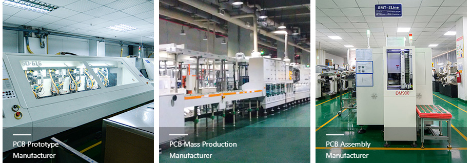
 PCB Assembly
 Layer Buildup
 SMD-Stencils
 PCB Design-Aid & Layout
 Mechanics
 Quality
 Drills & Throughplating
 Factory & Certificate
 PCB Assembly Factory Show
Certificate
PCB Assembly Factory Show
Certificate
Support Team
Feedback:
support@nextpcb.com


Following our previous architectural discussion in "What issues should be considered in the design of printed circuit boards", we are diving deeper into the foundational theory and practical execution of PCB design. In 2026, hardware engineering is no longer just about connecting dots on a schematic. To ensure a circuit board achieves its expected performance, the overall layout and routing strategy play a critical role. These factors directly dictate system reliability, thermal management, signal integrity, and the ultimate success of the manufacturing process.
The physical dimensions of your printed circuit board should be your first priority. When the PCB size is excessively large, trace lengths increase, leading to higher parasitic impedance, increased susceptibility to EMI (Electromagnetic Interference), degraded anti-noise capabilities, and inevitably, higher PCB manufacturing costs.
Conversely, if the board is too small, thermal dissipation becomes a severe bottleneck. Components are forced too close together, leading to thermal throttling and dangerous cross-talk between adjacent signal traces. Therefore, establishing a reasonable form factor based on the mechanical enclosure and panelization efficiency is paramount.
Once the outline is locked, begin by placing special components (like connectors, heavy transformers, and mounting holes) and defining functional unit circuits. According to the signal flow, the core component of each module (such as a primary MCU or FPGA) should act as the central hub. Other peripheral components must be arranged around it evenly, neatly, and compactly.
However, avoid packing massive components too closely. Provide adequate clearance (keep-out zones) around larger and taller components to facilitate automated placement, visual inspection, and potential manual rework. For high-power integrated circuits (ICs) or MOSFETs, a thermal management strategy is non-negotiable. Allocate sufficient space for aluminum heat sinks, thermal interface materials, or dense thermal via arrays. Place these heat-generating components in well-ventilated areas of the board, ideally near the chassis exhaust.
While density is important, over-concentration must be avoided. Distribute heavy components evenly to balance mechanical stress. Several large components on the same board should maintain an adequate pitch and often perform better when aligned perpendicularly or at a 45-degree angle to the wave soldering direction, depending on the specific assembly machine.
For surface-mounted devices (SMDs) like SOPs and QFPs, the components must be aligned uniformly. The longer axis of the IC should align consistently relative to the transfer direction through the reflow oven. If wave soldering is employed for mixed-technology boards, component orientation becomes even more critical to prevent "shadow effects"—a common defect where smaller components behind larger ones are starved of solder.
Adhering to these orientation constraints significantly reduces solder bridges, tombstoning, and dry joints during the PCB assembly (PCBA) process.
Additionally, ergonomic considerations govern user-interface components. Light-emitting diodes (LEDs), reset switches, jumpers, and potentiometers should be positioned securely along the board's edge or at locations accessible through the enclosure.
Finally, for high-frequency or same-frequency circuits, the parasitic distribution parameters between adjacent components must be strictly managed. Generally, routing components in parallel reduces crosstalk. However, at higher frequencies (GHz range), proper shielding, grounding, and maintaining a 3-5 cm clearance from the PCB edge for sensitive RF components is critical. The mechanical properties of the substrate—such as its Coefficient of Thermal Expansion (CTE), thermal conductivity, heat resistance (Tg), and flexural strength—must be evaluated to guarantee reliable turnkey PCB production without warpage.
After locking the position and orientation of the layout, the crucial phase of PCB routing begins.
Wiring must be executed efficiently. The golden rule is simple: traces on the printed board should be as short as mathematically possible. The more direct the routing, the lower the channel occupancy, meaning you achieve a higher pass-through rate (fewer layers required). Input and output wires must avoid running parallel over long distances to prevent capacitive or inductive feedback coupling. A classic mitigation strategy is to place a solid ground trace between the two sensitive lines, acting as a coplanar waveguide.
In multi-layer designs, the signal routing direction of adjacent layers must be orthogonal (e.g., Layer 2 routed vertically, Layer 3 routed horizontally) to minimize broadside crosstalk.
For critical signals, especially high-speed digital lines (USB, PCIe, Ethernet), the routing engineer must collaborate with the system designer. Differential pairs must be routed together, maintaining parallel, close spacing, and critically, equal electrical lengths to prevent phase skew.
The minimum width of standard PCB traces is determined by the required adhesion strength to the substrate and the continuous current it must carry (I2R heating). The general thermal guideline (simplified IPC-2152 standard) indicates that for an outer layer trace with 1 oz/ft2 (approx. 35μm) copper thickness and a width of 1.5mm, a continuous current of 2A will typically result in a temperature rise (ΔT) of no more than 10°C. While power traces benefit from massive widths, modern digital signals demand miniaturization.
| Current Application | Recommended Width (1oz Copper) | Notes |
|---|---|---|
| Low-Speed Digital/Analog (10mA) | 0.1mm - 0.2mm | Standard manufacturing process |
| High-Density Interconnect (HDI) | 0.02mm - 0.05mm (20-50μm) | Requires mSAP advanced fabrication |
| Power Delivery (2A) | 1.0mm - 1.5mm | Varies by acceptable ΔT |
| High Power Delivery (5A+) | Polygons/Copper Pours | Use thermal reliefs on pads |
Of course, whenever space allows, default to wider traces for power and ground networks to lower overall impedance. The minimum spacing (clearance) between lines is dictated by the breakdown voltage required and the limitations of the etching process. For standard logic ICs, clearances of 0.12mm (5 mils) are routine, but high-voltage sections must adhere to creepage and clearance standards (e.g., IPC-2221) which may dictate gaps of 5-8mm depending on the working voltage and pollution degree.
When routing corners, 90-degree right angles should be avoided. While the traditional "acid trap" argument is less relevant for modern alkaline etching, right angles create impedance discontinuities and impedance mismatches in high-frequency circuits. Use 45-degree chamfers or smooth, smallest-arc curves.
Historically, designers avoided large solid planes of copper foil, opting for grid-hatched (cross-hatched) patterns to prevent foil expansion and delamination under high heat. While modern high-Tg FR4 substrates handle solid copper beautifully, cross-hatching is still highly relevant for rigid-flex designs to maintain flexibility, or to dial in specific impedance values.
The terminal endpoint of any trace is the component pad. For through-hole components, the finished hole size (FHS) must be slightly larger than the device lead diameter (usually +0.2mm to +0.3mm) to allow capillary action during wave soldering. If the hole is too large, the solder cannot bridge the gap properly, forming a cold or "virtual" solder joint.
The outer pad diameter determines the annular ring. A legacy rule suggested a pad diameter (D) not less than (d + 1.2) mm for heavy hand-soldering. However, in modern 2026 manufacturing, achieving an annular ring of 0.15mm (6 mils) per side is standard practice. Thus, a pad diameter of (d + 0.3) mm to (d + 0.5) mm is optimal for densely packed, automated through-hole designs.
After defining the copper layer rules, the silkscreen overlay must be generated. The component outline and reference designators must be printed clearly. Generally, to ensure legibility during PCBA inspection, text height should be approximately 0.9mm to 1.5mm, with a stroke line width of 0.15mm to 0.2mm. Never place silkscreen characters over exposed copper pads, as the ink will contaminate the solder joint. If you are designing a double-sided board, remember that bottom-layer characters must be mirrored so they read correctly when the board is flipped.
The line between a functional prototype and a successful commercial product is Design for Manufacturability (DFM). By adhering to standardized manufacturing capabilities, engineers can significantly reduce the cost of their boards, turning what might have been an expensive prototype into a true low cost PCB without sacrificing quality.
Some crucial 2026 DFM strategies include:
When rapid iteration is essential, working with a responsive quick turn PCB provider ensures that your DFM checks are done promptly, avoiding days of back-and-forth communication before production even begins.
Consider a recent IoT gateway project requiring both high-current motor control (5A spikes) and a sensitive 2.4GHz Wi-Fi antenna on a tight 4-layer FR4 board. The initial layout placed the motor driver directly adjacent to the antenna feed line, causing massive EMI noise and connection drops.
By applying the routing rules discussed above, the team executed a redesign:
The result was a board that passed FCC emission testing on the first try and was perfectly optimized for turnkey manufacturing.
>> Why Choose NEXTPCB Manufacturer
For standard digital and low-power analog signals routing on 1oz copper, a trace width of 0.15mm to 0.25mm (6 to 10 mils) is typical. For power traces, widths should be calculated based on the maximum current; a 1A current typically requires at least a 0.3mm (12 mil) trace to keep the temperature rise negligible, though 1.0mm is safer for longer runs.
Clearance is strictly dictated by the voltage differential and environmental factors (pollution degree), as outlined in IPC-2221. For standard secondary circuits up to 50V, a 0.6mm clearance is often sufficient. However, for mains voltage (e.g., 220V AC), clearances must often exceed 2.5mm, and sometimes require routing slots (air gaps) to prevent arcing.
In high-speed digital and RF designs, 90-degree corners cause an abrupt change in the trace width at the corner, leading to a localized drop in characteristic impedance. This discontinuity causes signal reflections, degrading signal integrity. 45-degree chamfers or rounded arcs maintain a more consistent impedance profile.
A pad is an exposed area of copper (often plated with tin, gold, or silver) designed for a component pin to be soldered onto. A via is a plated hole used exclusively to route an electrical connection from one layer of the board to another, and it is usually covered by solder mask (tented) to prevent accidental short circuits.
To ensure a low cost PCB, stick to standard specifications: use a standard 1.6mm FR4 substrate, 1oz copper thickness, standard green solder mask, and white silkscreen. Avoid blind/buried vias and keep minimum trace/space above 0.15mm (6 mils) to avoid premium manufacturing upcharges. Designing for standard panelization also significantly cuts down per-unit costs.
Applying these robust layout and routing methodologies guarantees that your hardware will not only perform optimally but will also sail through the PCB manufacturing and assembly phases with minimal friction. For engineers looking to bring their complex layouts to life, partnering with an experienced fabricator is the final, crucial step.
Still, need help? Contact Us: support@nextpcb.com
Need a PCB or PCBA quote? Quote now


 Surface

