
 NextPCB Capabilities
Printed Circuit Boards
NextPCB Capabilities
Printed Circuit Boards
 PCB Assembly
 Layer Buildup
 SMD-Stencils
 PCB Design-Aid & Layout
 Mechanics
 Quality
 Drills & Throughplating
 Factory & Certificate
 PCB Assembly Factory Show
Certificate
PCB Assembly Factory Show
Certificate
Support Team
Feedback:
support@nextpcb.com


PCB crosstalk is a significant issue for engineers dealing with high-speed PCBs. With today's compact boards, analyzing crosstalk before assembly is crucial.
Crosstalk is a challenging issue for printed circuit boards, often emerging in a project's final phase and manifesting intermittently. Electronic designers must address potential crosstalk causes early on.
Crosstalk impact clock signals, periodic and control signals, data lines, and I/Os. It causes "fake" logic states and disrupts circuit operation. It can also introduce unwanted noise to analog signals. To tackle crosstalk, it's essential to understand its nature and apply effective strategies, especially in high-frequency circuits.
In this article,
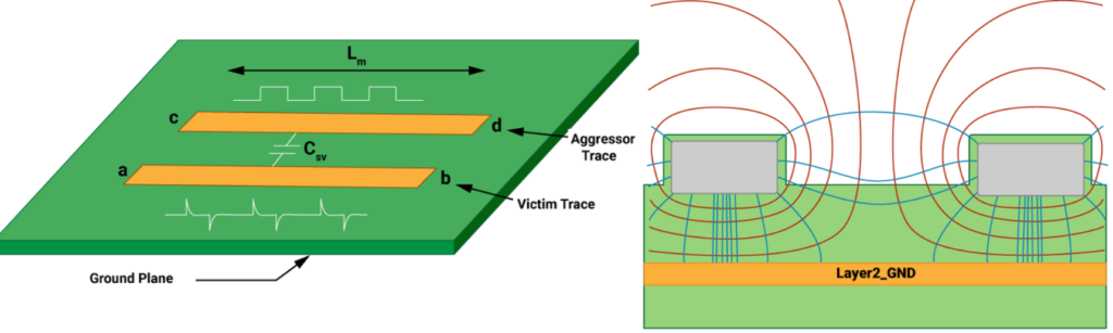
Crosstalk is the unwanted electromagnetic coupling between traces on a printed circuit board (PCB). It occurs when traces are too close, causing interference without physical contact. Two types of coupling exist: inductive (magnetic) and capacitive (electrical).
Inductive coupling happens when a current creates a magnetic field, inducing a voltage in an adjacent trace, potentially compromising signal integrity. Capacitive coupling occurs when an electric field generates a parasitic capacity, degrading signal integrity. Proper spacing and design can mitigate these issues.
To combat crosstalk, engineers and designers must focus on various strategies and design practices.
One common approach is to increase the distance between traces, thereby reducing the coupling effect. Another method is to use a ground plane, which helps isolate traces and minimize capacitive coupling. Additionally, using differential signaling, where two complementary signals are transmitted together, can cancel out noise and interference, improving signal integrity.
Designers can also utilize impedance control, which involves matching the impedance of traces to minimize reflections and signal distortion. This is particularly important for high-speed designs where signal integrity is crucial.
Based on Propagation Direction: Forward and Backward
Forward crosstalk, a straight path. Signals travel in the same direction as the aggressor signal. Backward crosstalk, a return journey. Signals propagate opposite the aggressor signal's direction. Different paths, same interference. Understand their paths and conquer crosstalk.
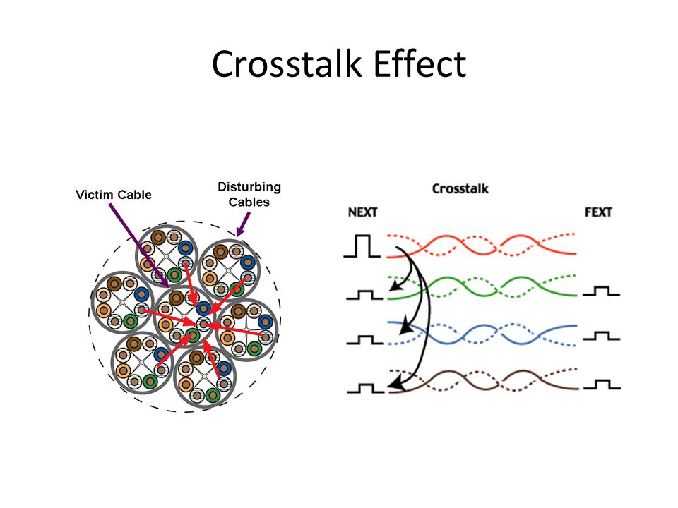
Based on Measurement Zone: Far End and Near End
The far end, distant trouble. Crosstalk measured at the receiving end of the victim trace. Near end, a closer foe. Crosstalk measured at the source of the victim trace. Unwanted coupling, regardless of distance. Recognize their zones and keep crosstalk in check.
Based on Quantification: PS FEXT, PS NEXT, and PS ELFEXT
PS FEXT, a quantified enemy. Power sum far-end crosstalk measures interference from multiple aggressors at the far end. PS NEXT, the nearby rival. Power sum near-end crosstalk measures interference from multiple aggressors at the near end. PS ELFEXT, the balanced bane. Power sum equal-level far-end crosstalk measures signal loss relative to far-end crosstalk. Quantify these menaces and optimize your PCB design.
Capacitive Coupling
Capacitive coupling, an unwelcome guest. This issue arises when traces on PCBs are too close. Electric fields from traces interact, causing interference. Signal quality declines. Prevention is vital. Designers must consider trace spacing and shielding techniques. By doing so, they combat capacitive coupling and protect signal integrity.
Inductive Coupling
Inductive coupling, the magnetic menace. When current flows in a trace, it produces a magnetic field. Close traces invite magnetic fields to interfere, inducing an unwanted voltage. Signal integrity is compromised. PCB designers must be vigilant. Proper trace routing and grounding techniques are crucial in the fight against inductive coupling. Keep your PCBs free from magnetic interference and safeguard their performance.
Common Impedance Coupling
Common impedance coupling, the shared foe. This type occurs when multiple traces use one impedance path. Currents intertwine, affecting each other. Signals become distorted. To counteract common impedance coupling, designers must avoid shared paths. Allocate individual impedance for every trace. In doing so, signal quality is preserved, and electronic devices can operate unimpeded. Let your electronics flourish, unburdened by this shared impedance threat.
The unwanted interference poses challenges for printed circuit boards (PCBs). But what impact does it have? We'll explore the effects of crosstalk on PCB design in this brief.
It is the bane of PCBs. Fear not, for we'll arm you with design guidelines to minimize this menace. Embrace these tactics and create crosstalk-free, high-performing devices.
Component Spacing
Component spacing is a simple solution. Keep components and traces at an adequate distance. By doing so, you reduce interference and signal integrity. Avoid congested layouts; embrace spacious designs.
Managing High-Speed and Sensitive Components
High-speed and sensitive components, demanding attention. Handle them with care. Keep these components apart from noisy, disruptive neighbors. Allocate separate ground planes for analog and digital signals. Crosstalk will recede, and your delicate components will thrive.
Avoiding Right Angle Bends
Right angle bends, a hidden peril. When routing traces, avoid sharp turns. They cause impedance mismatches and signal reflections. Instead, use 45-degree bends or curved traces. Crosstalk will fade, and your PCBs will deliver peak performance.
Thus, component placement and orientation are crucial for reducing crosstalk. Follow these best practices, and your PCBs will outshine the rest. Banish crosstalk, and let your electronic devices operate seamlessly.
Crosstalk is an unavoidable issue in high-speed PCBs. While it cannot be entirely eliminated, it can be reduced to maintain signal integrity and performance.
It occurs due to unintended coupling between parallel or adjacent traces. By properly spacing these traces, the coupling can be minimized. There are multiple methods to decrease crosstalk, so choose one that best suits your specific circuit design.
Still, need help? Contact Us: support@nextpcb.com
Need a PCB or PCBA quote? Quote now


 Surface

