
 Surface


Lolly Zheng- Sales Account Manager at NextPCB.com

 NextPCB Capabilities
Printed Circuit Boards
NextPCB Capabilities
Printed Circuit Boards
 PCB Assembly
 Layer Buildup
 SMD-Stencils
 PCB Design-Aid & Layout
 Mechanics
 Quality
 Drills & Throughplating
 Factory & Certificate
 PCB Assembly Factory Show
Certificate
PCB Assembly Factory Show
Certificate
Support Team
Feedback:
support@nextpcb.com


Introduction: Clarifying the Term and Scoping the Topic
In PCB manufacturing and design, “Mousebites” is a term that often causes confusion because it carries two distinct—yet visually similar—meanings in industry use. To provide a rigorous, clear analysis, we’ll first separate these two concepts and then define this article’s focus.
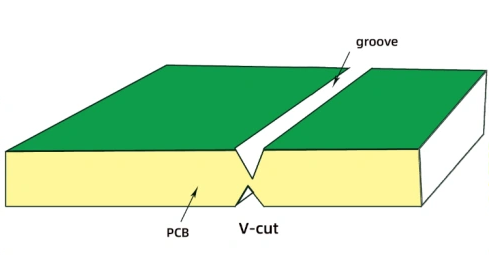
The first meaning, and the one more widely known across hardware engineering, refers to panelization breakaway “mousebites” in PCB assembly. This is a deliberately designed method for separating sub-boards. By drilling a line of closely spaced small holes along a narrow tab (tab routing) that links multiple PCBs, the tab’s mechanical strength is reduced. After assembly, operators can easily snap or tear individual boards from the panel by hand or with simple tools. This approach is cost-effective and flexible, especially for non-rectangular or irregular board shapes that are not suitable for V-scoring (V-CUT).
The second meaning, which is the core topic of this report, refers to an unintended microscopic surface defect. This “mousebites” shows up as a series of tiny, irregular notches, pits, or saw-tooth marks on key surfaces such as conductors, pads, or solder-mask openings. While its appearance resembles the rough edges seen after panel breakaway, its nature, root causes, and risks are entirely different.
Fundamentally, the two “mousebites” concepts reflect a deep contrast in PCB manufacturing: controlled, macro-scale mechanical weakening versus uncontrolled, micro-scale chemical/mechanical defects. Panelization mousebites are a useful, engineered tool with specified hole sizes and spacing to create a predictable weak point. Surface-defect mousebites are a process-control failure, typically tied to chemistry or micro-contamination. Distinguishing between the two is step one for effective quality control and root-cause analysis. This report focuses on the surface-defect meaning—its mechanisms, appearance and functional impact, acceptance criteria, and end-to-end prevention—so practitioners have a thorough reference.
Need a fast sanity check on manufacturability while you read?
Surface-defect mousebites rarely stem from a single cause—they are the combined effect of multiple weak controls across the PCB process. They are a textbook case of “upstream process issues manifested as downstream cosmetic defects.” The root causes trace back to several key stages.
This is one of the most common origins. In PCB fabrication, patterns are transferred by photolithography using dry film or ink, followed by etching to remove unwanted copper. Anything that blurs the pattern edge can create mousebites. For example, if dry film doesn’t laminate uniformly and tightly—leaving micro-bubbles, dust, or wrinkles—those spots won’t be protected during etching.
Etching control is also critical. Small drifts in etchant concentration, temperature, spray pressure, or conveyor speed can cause non-uniform etch rates. Over-etch near resist edges can bite into the copper, leaving tiny irregular notches—i.e., mousebites—along pads or trace edges. Exposure under-dose or over-development can also roughen the resist edge, predisposing copper to edge serrations in etch.
Designers & PE teams: use NextPCB’s free online Gerber viewer and DFM checks to spot edge-quality risks before fabrication.
As the PCB’s protective “skin,” solder mask integrity directly shapes surface quality. With LPI (liquid photoimageable) mask, mousebites can result from poor leveling, wrong viscosity, or uneven coating, which prevents a smooth, continuous film over fine copper edges. Under magnification, edges appear saw-toothed.
A more frequent driver is insufficient pre-clean. Residual contamination—dust, fingerprints, oxides—blocks adhesion, and after cure can leave tiny pinholes or edge notches. Incorrect prebake/final cure profiles (time/temperature) can cause uneven solvent evaporation or under-cure, compromising edge integrity.
If the copper surface has micro-discontinuities, subsequent plating or coating may not fully cover them. Process mis-settings can create micro-bubbles during electro/chemical deposition; bubbles shield areas from deposition and leave pits. Poor pre-treatment or wetting causes molten solder or plating solution to fail to spread, leaving “bitten” edges along metals or finishes.
> Recommend reading: PCB Surface Finishing 101: Processes, Pros & Cons
Some mousebites are mechanical. Aggressive or uneven brushing/deburring can nick copper. Incomplete rinsing after wet processes allows residual chemistry or particulates to re-deposit and dry into defects that look like mousebites.
Takeaway: a simple-looking mousebite often masks a compound cause chain. Example: poor surface cleanliness → mask leveling problems → tiny mask edge notches → finish can’t cover → base material exposed. Surface defects aren’t just inspection issues—they’re real-time indicators of process stability, and root-cause work must systematically weigh Man/Machine/Material/Method/Environment.
Mousebites are not merely cosmetic. They are a classic case where micro-defects trigger macro failures later in life.
Under 10×–30× magnification, mousebites appear as chains of tiny, irregular notches/pits along trace, pad, or mask-opening edges. Edges are rough and uneven; copper or substrate may be exposed. With side lighting, shadows enhance visibility.
To avoid confusion, distinguish mousebites from other surface defects:
| Defect | Morphology | Typical Location | Core Cause | Key Checkpoint |
|---|---|---|---|---|
| Mousebites | Chain of tiny, irregular notches/pits (saw-tooth edge) | Trace/pad edges, mask openings | Uneven etch, poor mask leveling, contamination | Copper/substrate exposure? Pad continuity impacted? |
| Pinholes | Tiny circular holes; may penetrate mask or substrate | Copper surfaces, pads, inside vias | Moisture in laminate; gas entrapment during via plating | Functional impact? Solder integrity? |
| Cratering | Cup/bowl-shaped depressions; sometimes white residue | Pad centers, under solder joints | Solder paste/thermal stress; laminate fracture | Voids/strength loss under the joint |
Solder success hinges on wetting—molten solder spreading uniformly to form an intermetallic layer. Irregular mousebites interrupt the wetting front, preventing full spread and causing poor wetting, opens/intermittents, voids, and weaker mechanical/electrical joints. In fine-pitch areas, edge notches can re-route solder flow, raising bridging/short risk.
Edge notches/sharp corners intensify electric field locally, becoming hazards in high-voltage/high-frequency designs—possible partial discharge, electromigration, or breakdown. If the substrate is exposed, especially in humid environments, effective creepage distance shrinks, increasing leakage/failure risk. Mask/finish gaps become corrosion initiation sites; under temp-humidity cycles, thermal shock, or salt spray, degradation accelerates, potentially leading to opens or drift.
A systematic, qualitative-to-quantitative workflow is needed, guided by industry standards.
IPC-A-600 (Acceptability of Printed Boards) is the globally recognized reference for bare PCB visual acceptability. It defines accept/reject criteria for features like conductive pattern width, etch characteristics, surface pits and nicks, with extensive figures and text.
IPC-A-600 defines three classes by end-use criticality:
> Recommend reading: IPC Class 2 vs 3: The Differences in PCB IPC Standards
Whether a small defect is acceptable depends on application criticality. A Class 1 toy may accept non-functional-impact defects; a Class 3 pacemaker board may reject even non-exposed cases due to lifecycle risk.
Work backward from effect to cause; link surface symptoms to specific process parameters.
This links appearance → process stage → data, forming a closed loop from detection to localization to correction.
Eliminating mousebites requires a closed-loop quality system from DFM to process control to outgoing inspection.
| Suspected Cause | Visual Symptom | Checks (Man/Machine/Material/Method/Env) | Prevention/Improvement |
|---|---|---|---|
| Uneven etch | Serrated trace edges; varying width | Method/Machine: etchant conc/temp/spray; Material: dry film quality, surface cleanliness | Optimize etch; calibrate tools |
| Poor mask leveling | Rough mask window edges; tiny notches | Method: ink viscosity/leveling time/cure; Env: cleanliness/RH | Adjust ink & coating; strengthen dust control |
| Finish defects | Discontinuous metal/film; “bitten” edge | Method: agitation/time; Material: bath activity/cleanliness | Thorough pre-treatment; improve wetting/agitation |
| Item | DFM Rule | What to Check | Why It Prevents Mousebites |
|---|---|---|---|
| Traces & pads | Avoid sharp corners/needle features; use fillets/teardrops | Teardrops on critical pads? Rounded corners? | Lowers field & stress concentration; improves etch/mask smoothness |
| Solder mask | Proper mask expansion & dam width per fab capability | Clearance between mask opening and pad edges | Prevents rough mask edges; lowers bridging risk |
| Panelization | Align breakaway and deburr specs with fab | Hole size/pitch, tab count/location agreed? | Ensures mechanical integrity; avoids later edge damage |
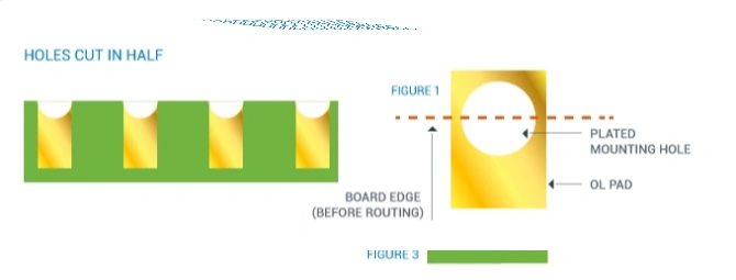
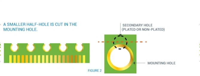
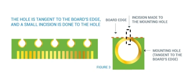
Here we briefly cover breakaway mousebites for completeness. Holes are drilled along breakaway tabs to form an easy-to-fracture line. After separation, the board edge retains a rough, “bitten” look.
Key design considerations:
Rough edges can cut operators or interfere with enclosures. Poor tab design can propagate microcracks into the board. Plan for secondary routing/chamfer/deburr after depanel.
As a PCB surface defect, mousebites are more than minor cosmetic flaws; they’re signals of process stability. Risks span the entire lifecycle—from solderability and electrical reliability to environmental durability under stress.
Eliminating mousebites requires a closed loop from DFM to process control to final inspection. Only tight cross-functional collaboration will ensure high quality and reliability in increasingly complex builds.
Ready to turn guidance into boards? — Get an instant quote, choose finishes, and add turnkey assembly at NextPCB.
Scaling after validation? — Use NextPCB’s quick-turn prototype, 24-hour PCBA, and certificate-backed QA to ramp confidently.
References:
[1] Lim, J. Y., Lim, J. Y., Baskaran, V. M., & Wang, X. (2023). A deep context learning based PCB defect detection model with anomalous trend alarming system. Results in Engineering, 17, Article 100968.
[2] He, Z., Lian, Y., Wang, Y., & Lu, Z. (2025). A comprehensive review of research on surface defect detection of PCBs based on machine vision. Results in Engineering, 27, Article 106437.

Still, need help? Contact Us: support@nextpcb.com
Need a PCB or PCBA quote? Quote now

