
 NextPCB Capabilities
Printed Circuit Boards
NextPCB Capabilities
Printed Circuit Boards
 PCB Assembly
 Layer Buildup
 SMD-Stencils
 PCB Design-Aid & Layout
 Mechanics
 Quality
 Drills & Throughplating
 Factory & Certificate
 PCB Assembly Factory Show
Certificate
PCB Assembly Factory Show
Certificate
Support Team
Feedback:
support@nextpcb.com


Gerber is a standard file format used in the electronics industry to describe the physical design of printed circuit boards (PCBs). It contains information such as the location and geometry of copper traces, silkscreen, solder mask, the board outline and drill holes on the PCB board, and can also be used to describe the dimensions and positions of all the components on the board. Gerber files are generated by electronic design automation (EDA) software and are used by PCB fabricators to manufacture the PCB board accurately. Gerber files can be viewed using a Gerber viewer software, with some specialist tools also allowing for the editing of Gerber files directly.
Already Have Gerber Files?
Try Our Free Online Gerber Viewer HQDFM - Free Desktop Version Download
This article will cover:
Before starting on the actual Gerber files generation process, it is important to recognize that while the overall export process is similar across PCB design tools (export Gerber files, export drill files, package into a .zip/.rar file), the resulting file structure, names and content may vary due to differences in design formats and software implementations. Each EDA tool handles the translation of PCB data into Gerbers differently and different PCB fabricators will have different preferences. Always verify with your manufacturer to see if they have any specific preferences when exporting Gerber and drill files.
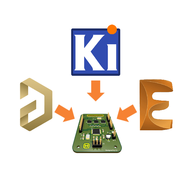
In this article, we will go through the Gerber export process for three mainstream printed circuit board design tools – Altium Designer, KiCad and Autodesk Eagle.
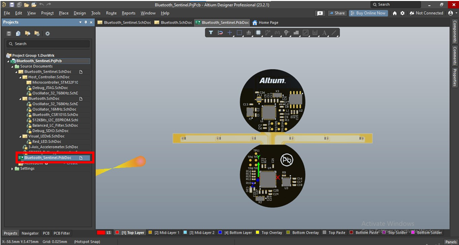
Step #1: In Altium Designer, open the .PcbDoc PCB layout file.
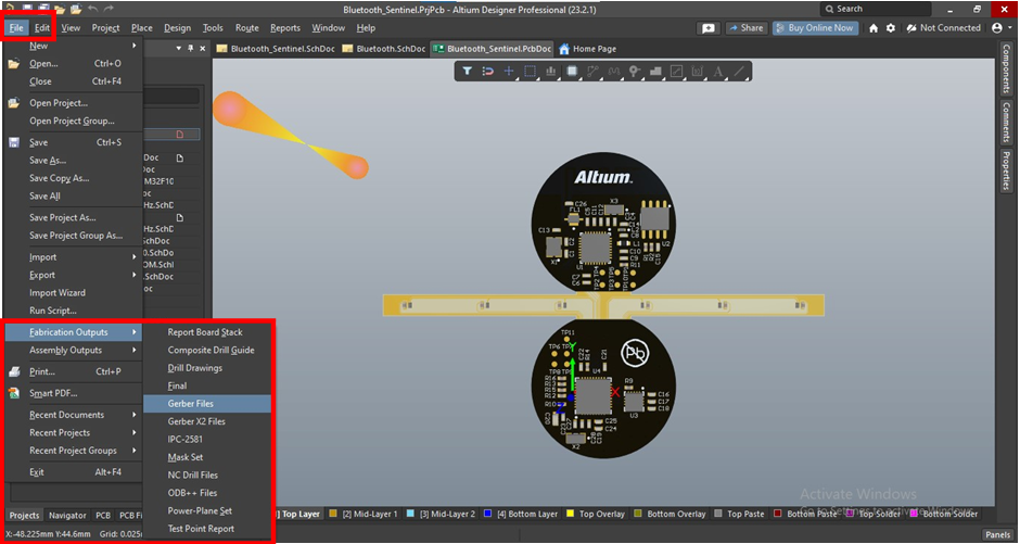
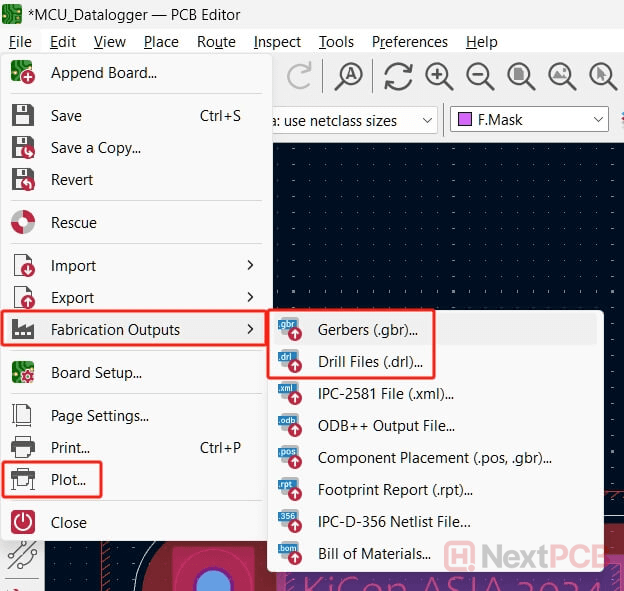
Step #2: Click File at the top left corner and select Fabrication Outputs and then Gerber Files from the drop-down menu.
Step #3: Choose between Inches and Millimeters for the units and the Decimal precision. For large, simple designs you may want to choose a lower precision for smaller file sizes. Complex, high-speed designs may benefit with higher precision.
For the Gerber filename, it is recommended to used the Protel filename extensions (filename.*(gtl, gbl, .gto,...) so viewers can better identify the layers.
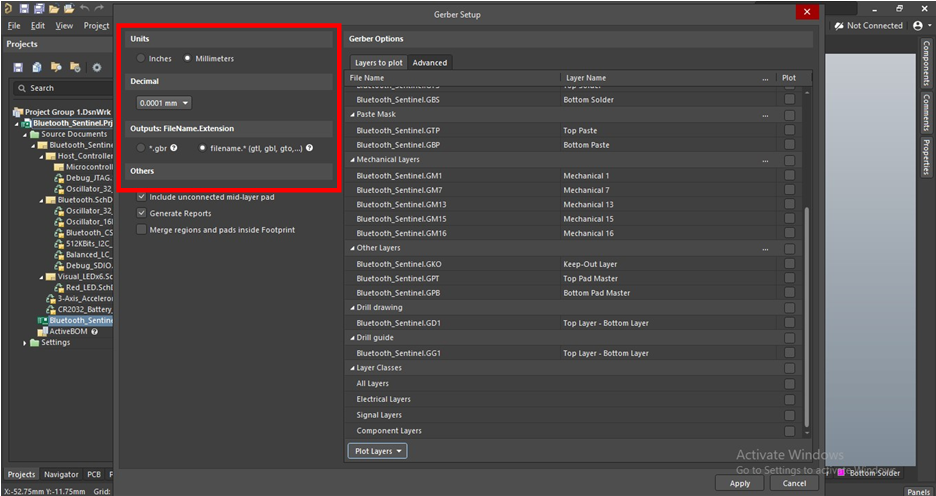
Step #4: Now it's time to select the layers to export. On the right side of the window, you can select the individual layers to export manually. However, at the bottom, there is an option to select only the layers used in the design. Do this by going to Plot Layers -> Select Used.
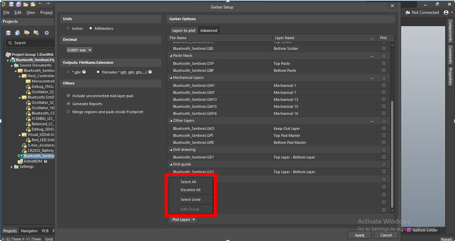
The Advanced tab contains more settings to configure however, the default settings work for most cases.
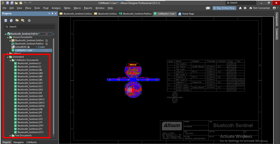
Step #5: Click Apply and the selected layers will be exported as Gerber files in the Altium Project Directory. Depending on your version of Altium, the exported files may be exported inside a folder called Project Outputs for [project name]. Altium will then open the CAMtastic file viewer for you to review the Gerber files, however, we need the Gerber files for production, not the CAMtastic.cam file. This project file is merely a container to save workspace data.
Now we have generated the Gerber files, we also need to generate the Drill Files that define the location and sizes of through holes, vias and other holes on the board. Since many drill machines typically accept NC (numerical control) data, the drill file is not actually a Gerber file and must be exported in a separate step.
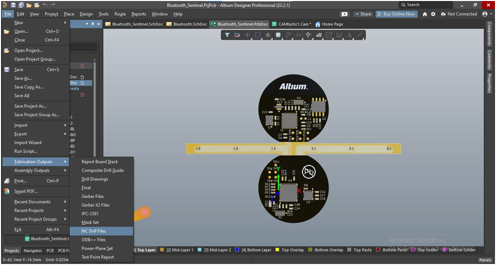
Step #6: To generate Drill Files, go to File -> Fabrication Outputs -> NC Drill Files.
Step #7: A new dialogue box will open. Keep the same units as before, follow the Other settings as shown in the below screenshot and click OK. Be sure not to check the Generate EIA Binary Drill File (.DRL) option unless specifically requested by the manufacturer as this is an older format that is not widely supported.
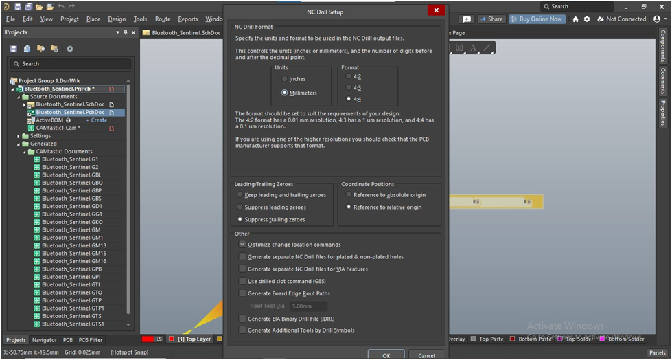
Tip: You may notice that some of the settings are similar to the settings in the Gerber export dialogue's Advanced tab. If your fab house or Gerber Viewer is having issues getting the drill holes and Gerber layers to align, ensure these settings are the same where possible. Most engineers and software can automatically change the settings so they align, however, some less common configurations can be harder to match.
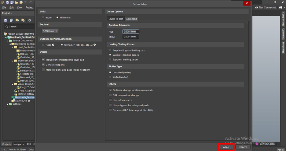
Step #8: Now, another small dialogue box will appear. Click OK.
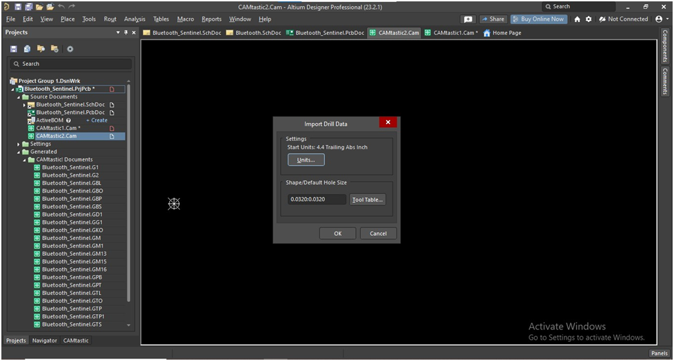
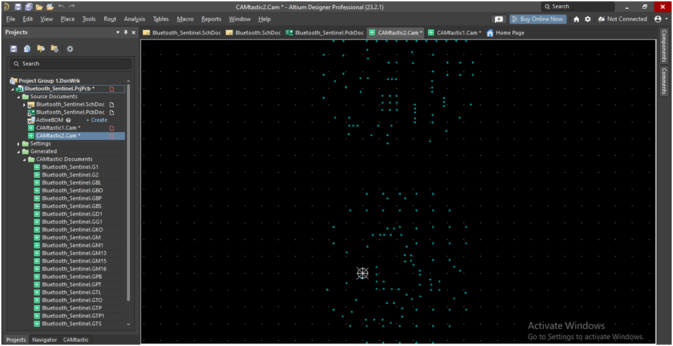
Altium will then export the files in the same directory and display the CAMtastic view of your drill file/files. The drill files used for manufacture will have the .TXT file extension and .TX1, .TX2, for multiple drill files. Other files such as the drill report (.DRR) and the drill pair report (.LDP) will also be generated and can be sent alongside the NC drill files to provide your manufacturer with additional information.
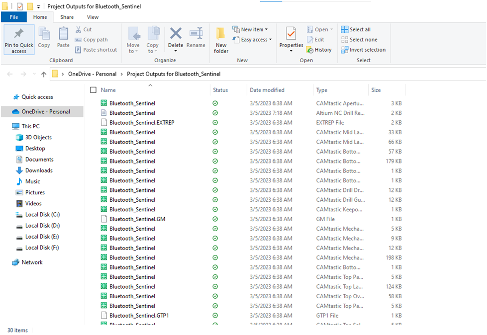
Tip: Set Windows to Show file extensions otherwise you will not be able to see many of the file extensions in File Explorer like in the screenshot below.
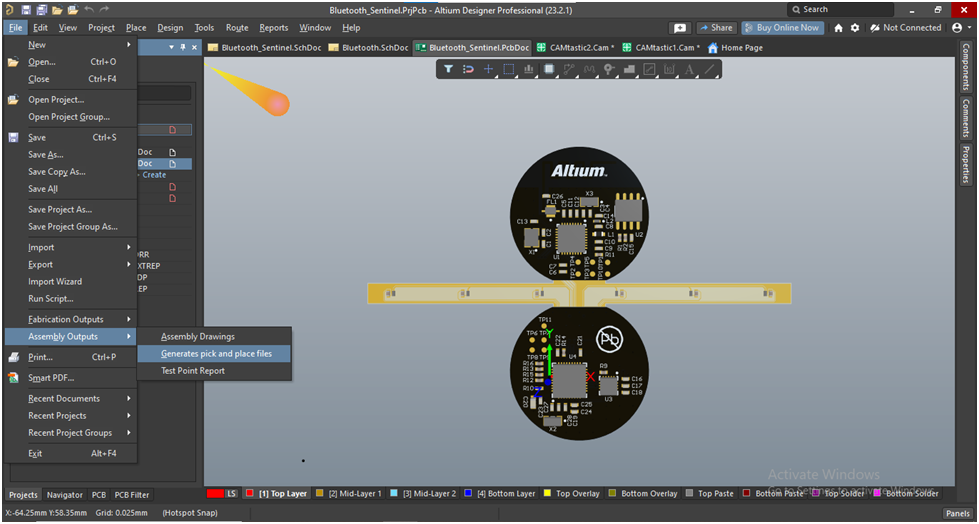
For automated PCB assembly, you may also need the component Pick and Place file that contains the location and orientation of all the components on the board. Contract manufacturers and turnkey PCB assembly providers like NextPCB may ask for this file.
Step #9: Return to the .PcbDoc file and go to File -> Assembly Outputs -> Generate pick and place Files
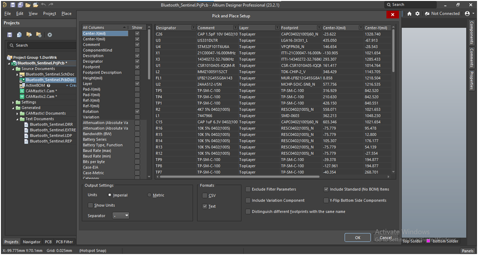
Step #10: The new Pick and Place Setup window will display a preview of the pick and place file where you can modify the headers and export options. Again, check with your assembly house to see what information they require and if they have any specific preferences.
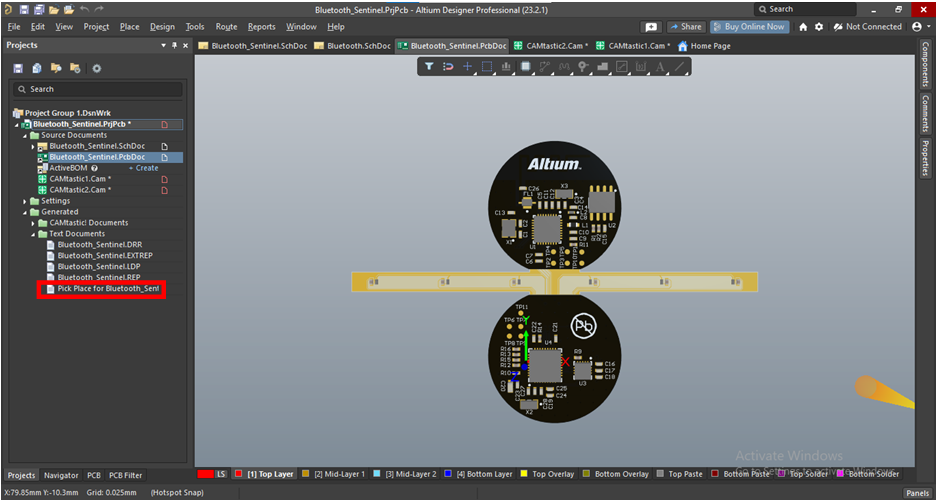
Step # 12: Click OK and the pick and place file will appear with the other exported documents under Text Documents.
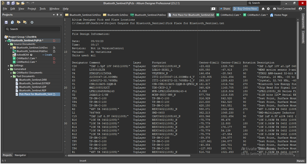
Double-click the file to see the contents
Now you have exported the necessary documents to produce your PCB. You can now package them into a .zip or .rar archive file and but before you send them to your manufacturer, we strongly advise checking the files in an external Gerber viewer software. The Altium Camtastic Viewer gives you a preview of the exported files in Altium, however this is not necessarily the what is in your archive file. CAMtastic is also an old tool which has not seen a major update for many Altium generations.
Use a third party Gerber File viewer like HQDFM to review your Gerber files and perform free Design for Manufacture (DFM) review to reduce board respins, improve reliability and eliminate unncessary production costs. Download the free desktop version for full DFM and DFA (Design for Assembly) capabilities and PCB manufacturing tools such as the quick Gerber panelizer and footprint checker or try the online Gerber Viewer version for convenience.
> Get Practical DFM Checklist and HQDFM Practice
In comparison, the Gerber export process in KiCad is much simpler. Just select the desired Gerber layers and generate the drill file.
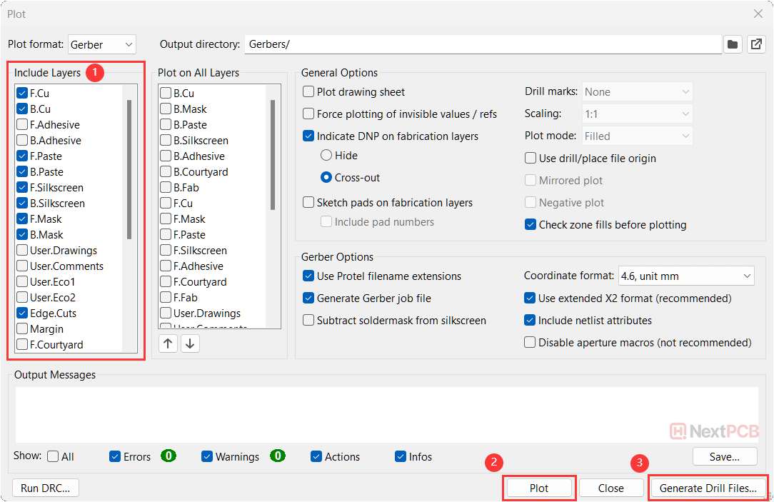
Step #1: Start by opening the PCB layout file (.kicad_pcb). Then go to File -> Plot or click the plot icon from the main toolbar. You can also go to Fabrication Outputs -> Gerbers (.gbr)...
Step #2: This will open up the Plot dialogue. Select the layers to export on the left and copy the other options unless specified otherwise.
Here is a list of essential layers required for a double-layer PCB and their KiCad (Protel) filename extensions:
For multilayer PCBs, remember to check the inner copper layers as well and if you require stencils, be sure to include the paste layers (F.Paste and B.Paste) as well.
Click the Plot button to generate the selected Gerber files.
Step #3: Now we have the Gerber files, remember we still need to export the Drill Files. To do so, click the Generate Drill File button on the bottom right.
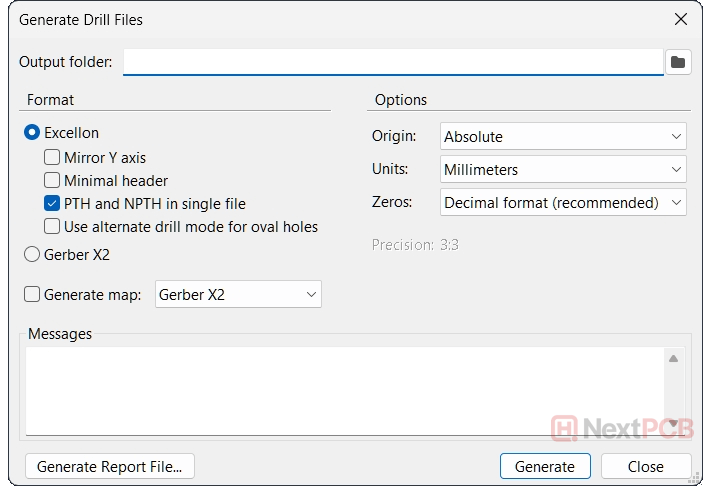
It will open up another pop-up window with the name Drill Files Generation. At this stage, it is recommended to use the default settings. However, you can make changes as per your requirements. From the Drill File Options check the Merge PTH and NPTH holes into one file option and hit the Drill File button on the left side of the window.
Step # 05: After hitting the Drill File you will be directed to the Plot Window there click Close at the bottom right of the window and you are done with generating your PCB Gerber Files.
Step # 06: So the last step of this process is to check your Gerber Files to verify whether everything is appropriate. To do so, KiCAD includes a gerber file viewer called GerbView, which allows users to preview circuit board's appearance before forwarding it to a manufacturer.
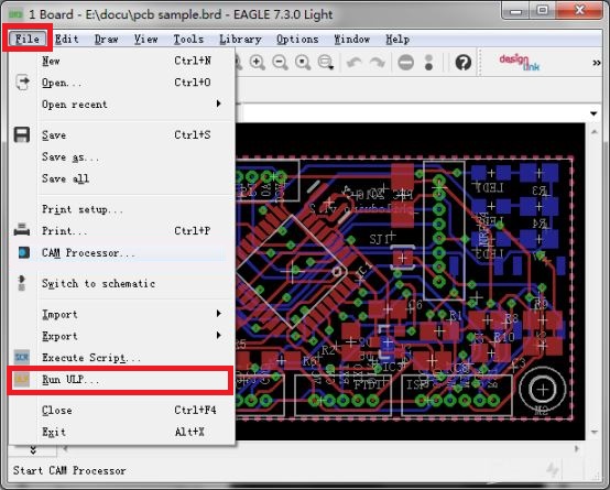
Step #1: The first step to generating Gerber Files in Eagle is to generate a Drill File. To do so navigate to the top-left side of the menu bar and click "File" then "Run ULP".
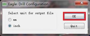
Step #2: A dialogue box will appear with a toggle consisting of two options mm and inch. Select inch and click OK. This will generate the drill file.
Step #3: Now, go to File -> CAM Processor...
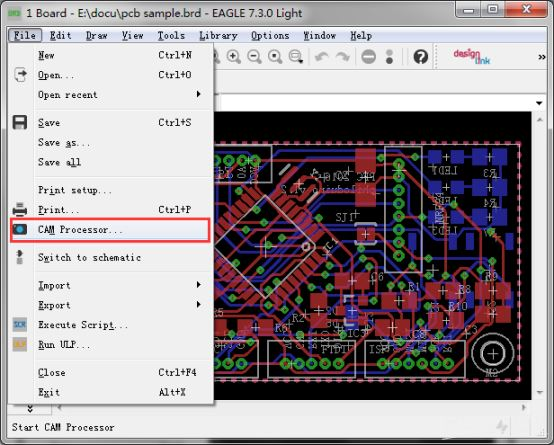
This will bring up the CAM Processor dialogue
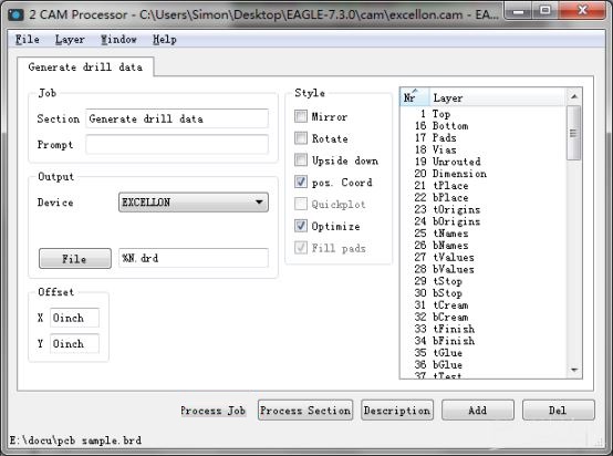
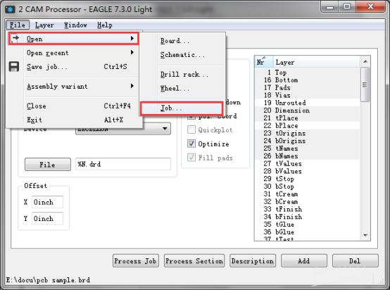
Step #4: Now, click the File at the top right corner of the window and then Open and select Job.
Then select Excellentone.cam and then hit the open button.
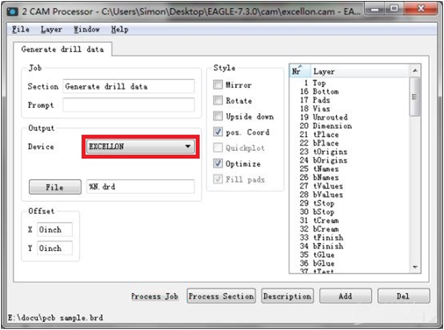
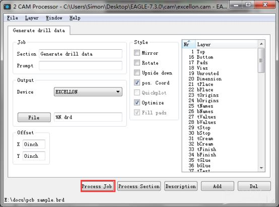
Step #5: Now click Process Job at the bottom of the window
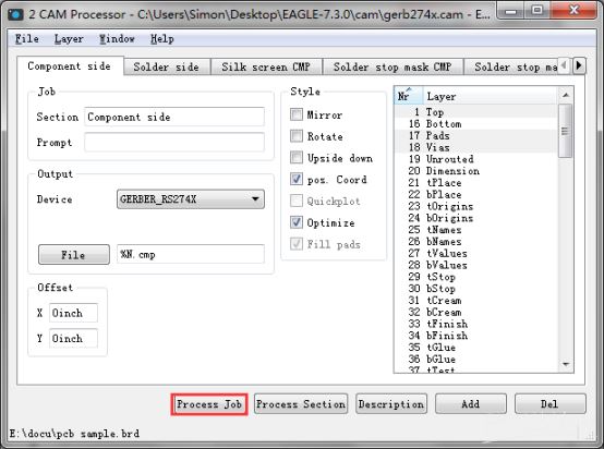
Step #6: Now, again in the "CAM Processor" popped up window, hit File then Open then Job, from the drop-down menu select GERBER_RS274X and click Process Job to generate the Gerber file
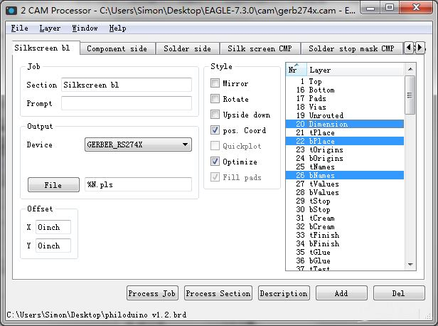
NOTE: 1) If your circuit board has double sided silkscreen layer, then you have to add it individually in the CAM Processor. To do so before processing the Job Click Add at the bottom right of the window then select 20 Dimension, 22 bPlace and 26 bNames
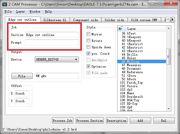
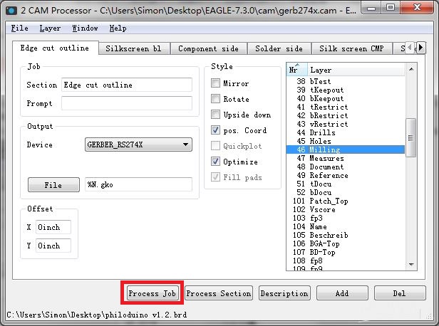
2) If you have any milling in your design you will also need the export the 46 Milling layer into the outline Gerber layer. To do so, click the Add button, change Section under Job to Edge cut outline and then select 46 Milling and 20 Dimension layers.
Once these steps are completed hit the Process Job button.
All the related files will be saved in the .brd file when the directory is.
Step #7: File Compression. As always, the exported files need to be packaged in an archive file to facilitate transfer. Windows and macOS systems have built-in tools to compress files into .zip files or you can use third party programs like WinRAR or 7-Zip. Once done, remember to check the Gerber files using a Gerber Viewer like HQDFM before forwarding it to your PCB manufacturer.
Texts elements are one of the basic components found on a circuit board. They are used to describe components, logos, draw symbols, etc. Text can make it easier to understand a printed circuit board visually. But writing on a PCB is not like writing on a piece of paper. Text elements are traditionally printed on the surface of printed circuit boards using a silkscreening technique, hence the name silkscreen.
In the process of exporting Gerber data, text elements may appear differently depending on the nature of the text. Eagle has options to create text using Vector, Proportional or Fixed fonts, with proportional being the default. However, when converted to Gerber data, the output is converted to vector format, which could lead to some unexpected surprises, a simple example of why it is important to review the Gerber files, not just the original design.
Gerber files consist of all the necessary information to manufacture a basic printed circuit board, including the placement of components, the size and shape of the board, and the routes that the electrical signals should follow. This information is crucial for the manufacturer, as it guides them to plan the manufacturing process and ensures that the PCB is made correctly and functions as intended.
Now that you understand what Gerber files are, it’s easier to emphasize their fundemental role in PCB manufacturing. Without them, producing a functional printed circuit board would be extremely difficult. Without proper Gerber files, manufacturers would need to rely on manual measurements and calculations, a process prone to errors and inefficiencies. This could lead to defective PCBs or even serious safety risks.
For these reasons, Gerber files - and other production formats are indispensable since they guarantee the proper functioning and safety of electronic devices.
Mastering the generation of Gerber files and Drill files is the critical bridge between your digital PCB design and a physical product. As demonstrated, while the interface differs between Altium Designer, KiCad, and Autodesk Eagle, the fundamental goal remains the same: accurately translating your design intent into a universal format that manufacturers can understand.
Remember that clicking "export" is not the final step. Different software versions and configurations can occasionally lead to output errors or layer misalignments. Therefore, it is essential to verify your data using a dedicated third-party Gerber viewer before sending your files to the fabrication house. By following the specific export steps for your EDA tool and performing a final DFM (Design for Manufacturing) check, you can eliminate interpretation errors, reduce the risk of costly board respins, and ensure a smooth manufacturing process.
NextPCB provides PCB manufacturing and assembly services, focusing on reliability without breaking the bank. With 5 factories in China and over a decade of quick turnaround electronics manufacturing from prototype to mass production, NextPCB serves over 160 countries around the world, pairing dependable electronics hardware with exceptional service.
For over 15 years, NextPCB has provided one-stop solutions for PCB manufacturing, assembling, and engineering services. We strive to utilize the latest technology and Industry 4.0 optimization to manufacture complex to high-level circuit boards and offer a wide range of PCB types, including metal-core, flex, rigid-flex, thick copper, HDI, LED, High-frequency, High-Speed, Waterproof PCBs and more.
Get in touch, learn about our PCB capabilities or get an instant PCB quote.
Still, need help? Contact Us: support@nextpcb.com
Need a PCB or PCBA quote? Quote now


 Surface

