Printed circuit board (PCB) fabrication turns design data into a reliable, production-ready board through a tightly controlled sequence of steps—DFM checks, imaging and etching, multilayer lamination, drilling and copper plating, solder mask and legend, surface finishes, profiling, and 100% electrical test. This guide walks you through the PCB fabrication process step by step and shows where tools like a Gerber viewer and DFM analysis fit in, so you can hand off clean final artwork (Gerber files), avoid rework, and get boards built faster with consistent quality.
Note: in this guide, “PCB fabrication” means producing the bare board (as governed by IPC-6012/IPC-A-600), while “PCB manufacturing” refers to the broader, end-to-end flow that also includes assembly into a functional PCBA (accepted under IPC-A-610/J-STD-001).
What is PCB Fabrication
Printed circuit board (PCB) fabrication is a process of fabricating real-life electronic printed circuit boards. The PCB fabrication follows a complex procedure that involves several steps that work together to make sure that the PCB functions well. Mainly the PCB is divided into two categories single or double layers and multilayers. The fabrication process for single-layer and double-layer PCBs is similar and simple. However, the fabrication process of multilayer PCBs is a bit complex and requires special knowledge and experience to design and fabricate. Hence, complex multilayer PCBs may involve up to 20 steps for fabrication. Modern PCB design often starts with powerful tools like KiCad, Autodesk Fusion 360 or Altium Designer, streamlining the transition from concept to production.
Each step in the PCB fabrication process is critical and requires skilled hands to execute. Minor negligence in the fabrication stage can negatively affect the performance of the PCB. Due to the accuracy needed for the fabrication process and the importance of proper handling, it is crucial to select an experienced PCB manufacturer that provides a wide range of services like NextPCB. At Next PCB, we perform multiple quality checks on our manufactured PCBs to ensure the delivery of a well-functioning circuit board.
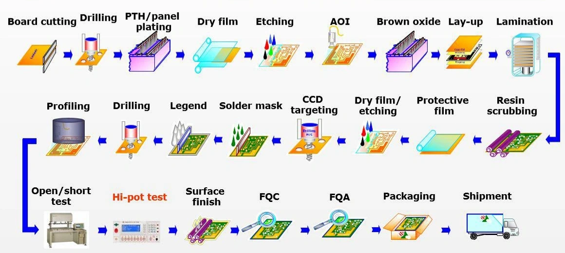
To aid your understanding of the PCBfabrication process, NextPCB has provided a flowchart that visually describes the stages of the process.
As mentioned, the PCBfabrication process involves several stages depending on the complexity and unique features of the circuit design. Understanding the fabrication process helps designers develop a deep knowledge of how PCB fabrication impacts the performance of the circuit board.
An understanding of the PCB fabrication process and its impacts on the output enables PCB designers to utilize such techniques that go well with the fabrication process. So, now that we know the importance of being familiar with the procedure of PCB production. Let's get its in-depth knowledge.
1. Schematic Design
Schematic design is the first stage of PCB production. In schematic design, the engineer outlines the building blocks of the various circuits integrated on a PCB. A schematic design narrates from where an electrical signal begins, where it connects with other components, and where it ends. The schematic uses symbols to represent electronic components, which help layout designers draw the blueprint of the printed circuit board. This initial phase demands top-tier schematic design software to ensure clarity and functionality.
2. Design PCB
After the completion of schematic drawings, PCB designing begins. PCB designing starts with complete planning and appropriate know-how of the functions of the circuit board, as the design parameters of a circuit board affect its electrical properties. The designer starts drawing a layout design by following the schematic drawings. The layout is the second stage of PCB production; it begins with outlining and declaring the board size and involves component placement on the board.
During component placement, the designer ensures that all the components are arranged in a way that avoids signal crossing. After placing the component, the designer creates a netlist by assigning each pad its dedicated net. A netlist may describe logic, connections between components, and hierarchical relationships. Further, the netlist helps in structuring the circuit board.
After the placement of components and generation of the netlist, it's time to route the signal traces. Now at this stage, the designers have two options for routing the PCB. Number one is auto-routing, which is possible due to netlist, and offered by the PCB layout software; the other one is manual routing which a designer does by himself to meet specific design parameters. During routing, engineers commonly employ trace analysis tools like the trace width current calculator to optimize copper trace dimensions for current handling, ensuring reliability.
To lay out the PCB blueprint, the designers have a wide range of PCB designing software, for example, Altium, Altium 365, Extended Gerber and Fusion 360.
3. Testing of Layout
Once the routing of the PCB is complete, the designer checks it against the schematic and all other aspects of PCB designing. This step ensures that there are no errors, as it's nearly impossible to modify the design after PCB fabrication starts. Any mistakes in this stage can affect the final output. Hence, the designers check them in different ways to find and eliminate the error, if any.
As soon as the testing gets ends, the Gerber file of the circuit design is sent to the PCB manufacturer, where the actual fabrication begins. When the PCB design file arrives at the fabrication house, the manufacturer first checks the file for the Design for Manufacturing (DFM) test to ensure the design meets the minimum fabrication requirements for the circuit board or not.
NextPCB's Gerber Viewer is an essential tool that allows PCB designers and engineers to view and analyze Gerber files, ensuring the accuracy and correctness before fabrication. This free online tool offers convenience and confidence in the PCB fabrication process.
At this stage, the manufacturer starts by printing the Gerber files onto laminates. But before getting printed onto the laminates, the Gerber files are printed onto a transparent sheet and make "films" known as the photo negatives of the PCB design or photo tools.These tools are printed using a plotter, which uses clear and black inks to differentiate the conductive paths and non-conductive spaces on the PCB. This step is foundational to the pcb production workflow.
Clear Ink: The plotter use clear ink to print the conductive paths of the printed circuit board.
Black Ink: The area printed with black ink refers to the non-conductive space of the PCB.
Note: For some reason, the functionality of ink is inversed for the outer layers of the PCB. This means that for outer layers, the clear ink denotes the area required to remove, while the black ink denotes the conducting paths of the circuit.
The number of films required for a PCB depends on its layer count. However, for the printing of the solder mask, the solder mask needs its "films." So, for a two-layer PCB, we need to print four films, and for a 4-layer PCB, we need to print six films.
Once the printing of films is complete, the manufacturer aligns all the photo tools and punches some holes through them, known as registration holes. Later these holes help align the photo tools with the laminate and fibreglass sheets.
5. Inner Layer Lamination
Lamination is a stage in PCB production at which the manufacturer stacks the copper layers, prepreg and laminates together and aligns them between two thick plates of steel and screws that plates together to generate pressure. Then the ready stack rests in a high-heat oven for curing, which is a process that melts the prepreg, so it works as an adhesive to bind the cores and copper layers together.
But before lamination, the laminates undergo a lengthy procedure consisting of several processes. So, let's have a look at them.
5.1 Inner Layer Image Expose
So, once the photo tools are printed, they are ready to get converted onto the laminates. Before the conversion of photo tools onto the laminates, the laminates are pressure washed to eliminate any dust or dirt to avoid issues like short circuits and open circuits. Then a coat of photo-sensitive material known as photoresist is applied to the laminate.
Now, to convert photo tools onto laminate, the manufacturer uses a UV printer. The UV printer has pins on its surface that works as a guide to align the photo tools with the laminate, as the laminate and photo tools have holes punched into it previously. Now, on the printer surface, the operator sandwiches a laminate between two photo tools and then lid down the printer. Then the printer starts its operation, and the area of photo tools printed with black, which represents the non-conducting parts of the circuit, absorbs the UV light and remains un-harden. Whereas the conducting surface of the circuit board, which is printed with clear ink, lets the UV light pass through it and gets polymerized or hard.
5.2 Inner Layer Image Develop
At the stage of image development, the UV-exposed laminates are pressure washed with an alkaline solution that removes the unharden layer of photoresist material from the laminates.
5.3 Inner Layer Etch
After removing the unharden layer of resist, the laminates are again pressure washed with an alkaline solution that etches the exposed copper from the laminates. Now at this stage, we get the exact same circuit design printed onto the laminates as we lay out in the software.
Cu2+ has oxidizing property in CuCl2 before etching and reacts with copper on the plate to reduce to Cu+
Chemical equation
Cu+CuCl2=Cu2Cl2
Cu2Cl2 is insoluble in water, but complexation can occur in the presence of an excess of Cl-
Cu2Cl2+4Cl- = 2 (CuCl3)2-
5.4 Resist Strip
After the etching, the dry film is chemically removed from all over the laminate, which leaves the whole circuit exposed.
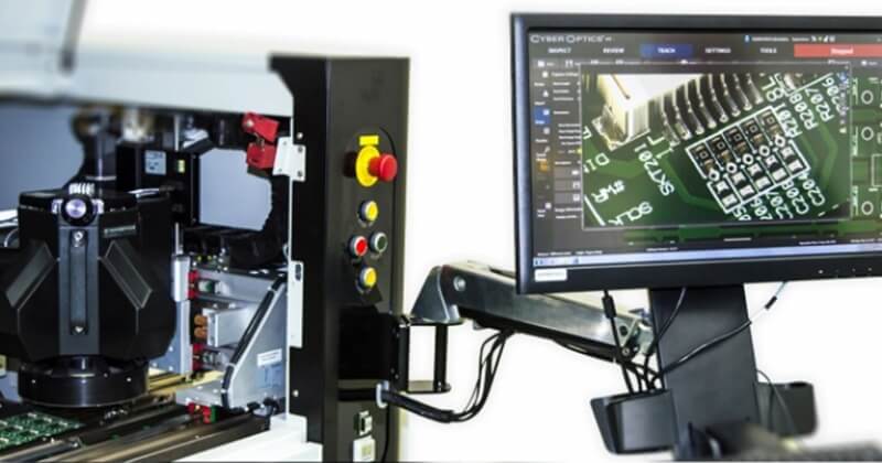
5.5 Inner Layer Automated Optical Inspection(AOI)
Before processing the finished laminate for drilling, it is significant to confirm that there are no errors in the laminates because, later, it is almost impossible to make changes in the inner layers of the PCB. To eliminate human errors, the manufacturer uses Automatic Optical Inspection(AOI). The AOI uses data provided by the Gerber files to check for errors. If any error is found, it is immediately shared with the concerned department to correct the mistake. Otherwise, the process of PCB fabricationcarries on without any disturbance.
5.6 Brown Oxide (Oxide Coating)
If the PCB is a multi-layer printed circuit board, after the Automated Optical Inspection and prior to the lamination, the inner laminates are chemically treated to make the surface of the laminates a little rough to aid the adhesion of the laminates during the curing process and increase laminate bond strength. At NextPCB, we use organic chemistry to oxide the laminates, which leaves the copper a dark brown in colour. However, there are other methods available too, that provide different colours.
The Aims behind Brown Oxide.
(1) Roughening the copper surface to increase the surface area in contact with the resin.
(2) Increase the wettability of the copper surface to the flowing resin.
(3) Make the copper surface passivated to avoid an adverse reaction.
5.7 Laminated Panels
The lamination is the process of binding cores, prepreg and copper foil together under high heat and high pressure. At this stage, the high heat melts the prepreg, and pressure helps the laminates to bond together and make a strong bond. After the lamination, we get a perfectly stacked board.
6. Drilling
After the lamination, the panel is ready for drilling vias and holes for through-hole components. Before drilling the holes, an X-Ray machine is used to locate and mark the spots where holes have to drill. Once the marking is complete, the laminates go for drilling. To avoid errors, the drilling of holes is a computerized process.
The normal-size holes are drilled with the standard machinery, but drilling tiny vias and holes requires special machinery. This accuracy is key in pcb board fabrication, especially for multi-layer units.
7. Deburr
The drilling process causes some uneven raised in the edges of the metal. Burr represents the same elevated copper. Whereas the deburr is the mechanical process of smoothing the elevated copper area. This process also clears the holes from the burr and provides smooth holes for electroplating.
8. Desmear
Desmear is a process of removing a thin layer of resin that usually appears on the inner copper layers due to heat and drilling. The desmear only applies to multi-layer circuit boards and enhances the electrical connectivity of the signal traces.
A more comprehensive answer to why we should execute desmear is that it exposes the copper rings that need to be interconnected in each layer. Further, the bulking agent can improve the pore wall structure and enhance the adhesion of copper plating.
KMnO4 is an important desmear raw material known as a debinding agent.
9. Electroless Deposition of the Copper
After the deburr and desmear, the walls of the holes become unconducive, which is why electroless copper deposition is necessary. Electroless copper deposition refers to the depositing of a specific amount of copper onto the walls of holes through a chemical process to make them conductive. The thickness of electroless copper deposits ranges between 45-60 millionths of an inch (microinch).
10. Outer Layer Lamination
The process of handling the outer layers of the printed circuit board is the same as for the inner laminates. The outer layers use the same photoresist that the inner layers use. The photoresist material covers the entire board, including the drilled holes and vias.
11. Outer Layer Expose
Similar to the inner layer exposed.
12. Outer Layer Develop
Similar to the inner layer development.
13. Copper Plating (Copper “Pattern” Plate)
Copper plating is a process of depositing copper on the exposed copper circuit through an electrical process. The thickness of deposited copper depends on the needed final finish of the circuit board. However, the most commonly deposited amount of copper is 1mil (0.001).
14. Tin Plating
After the electroplating of copper, the manufacturer electroplates tin on the exposed copper circuit. So now, the question is, why do we need to electroplate tin on top of copper? The tin works as etch resist during the etching of the outer layers. This means that during etching, the alkaline solution will only be able to dissolve tin, and the copper beneath the tin will remain intact.
15. Resist Strip
At this stage, we remove the developed photoresist from the outer layers of the circuit board; that we applied in the previous step. While removing the resist, the tin plating remains intact. After removing the resist strip, all the holes covered through it are now clean. It is the first step in the SES (strip-etch-strip) process.
16. Etch
After removing the resist strip, NextPCB etches the exposed copper area that the tin was not covering. By the end of the etching, we only have the pads and signal traces of copper covered with tin plating.
17. Tin Strip
At this stage, NextPCB also removes the tin plating through a chemical process, which leaves the copper beneath it exposed. It is the last step in the series of the SES (strip-etch-strip) process.
18. Clean and Prep for Solder Mask
After the Strip-Etch_Strip process, for better electric connectivity, before applying the solder mask, it is necessary to confirm that all the signal tracks, pads, through-holes and vias are clean and free of oxidation. When cleaning the laminates, the manufacturer also scrubs the panels with pumice to remove oxidation and make the laminates a bit rough to enhance the adhesion of the solder mask.
At this stage, the finished panel is coated with a liquid photo-imageable solder mask that thoroughly covers the laminate. After the application of the solder mask, the PCB is dried but not fully cured and exposed to intense UV light using a film tool. Then the PCB goes through another process that exposes the copper pads and holes.
20. Solder Mask Cure
There are many methods available to cure solder masks. But the most commonly used method is baking the PCB in an oven. The main purpose of solder mask application is to limit the area for solder masks and make a barrier between the copper circuit and the external environment to prevent copper from oxidation. Solder mask also prevents electrical shorting in the circuit during assembly and operation.
At NextPCB, legend or nomenclature would be screened on the panels before further processing. Also, at NextPCB, the nickel and gold plating for edge connectors ensues right after the final cure of the solder mask and legend. occur
Several processing options are available that can be done depending on the preferred final finish. Right now at NextPCB, we are providing our clients with an SnPb known as lead-free solder finish, Electroless Nickel Immersion Gold (ENIG), hard gold, immersion tin, and or immersion silver. Other finishes contain soft or bondable gold, Organic Solderable Preservative (OSP) and many other interesting and less-known finishes for instance palladium. Otherwise, the “Normal” processing would continue with the application of solder. This customization underscores the flexibility in circuit board fabrication under pcb standards.
21. Silkscreen (Legend, Nomenclature)
Silkscreen is the process of printing relevant information, such as the component number, placement position and company logo on the PCB. The silkscreen requires a specific ink. This specific ink usually has a standard colour of white, but the colour may vary according to the requirements.
22. Finishing the PCB
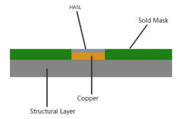
Standard printed circuit boards (PCBs) possess a copper layer on the circuit board. To prevent the copper layer from oxidation and damage, it is necessary to protect it. Otherwise, it will affect the quality of the performance and subsequent soldering. The method that the manufacturers used to protect the exposed copper pads and holes is simple and called surface finish. There is a variety of surface finishes available but the most commonly used protective layers are: hot air levelling (HASL), organic coating (OSP), electroplated nickel gold (plating gold), chemically immersed nickel gold (ENIG), gold finger, immersed silver (IS) and immersed Tin (IT) and so on.
It is a type of finish for PCBs in which the whole PCB is supposed to dip in melted solder so that the exposed copper gets enough coat of solder. However, during this process, some exposed copper areas get excessive solder coating, which is later removed by passing the PCB through hot air. The PCB experience hot air with intense pressure from both the front and back sides. This blast of air melts and removes the excess copper and levels it by spreading it all over the surface.
There are two types of Hot Air Leveling, lead and lead-free. However, only lead-free Hot Air Leveling is RoHS compliant[1].
Advantages: The advantage of using HASL or HAL is that it is low cost, and solderability is maintained throughout the fabrication process.
Organic coating PCB finish involves coating a liquid organic compound on the exposed copper that bonds with it and preserves it until the soldering. The organic compounds used for OSP usually belong to the azole family. For example, benzotriazoles, imidazoles, and benzimidazoles.
Advantages: comparable in cost with HASL, good coplanarity, lead-free process, RoHS complaint.
22.3 Electroplating nickel gold (plating gold)
This surface finish involves depositing gold on the exposed holes and pads through electroplating.
Advantages: good solderability, flat surface, long storage life, can withstand multiple reflow soldering and provides excellent resistance against oxidation even under unsuitable environments.
22.4 Electroless nickel and gold plating (ENIG):
This surface finish involves the non-electric depositing of nickel/gold on the exposed copper. Electroless nickel and gold plating surfaces serve longer than plating gold. [HASL vs ENIG]
Advantages: good solderability, flat surface, long storage life, can withstand multiple reflow soldering.
Gold finger: The edges of the connector, known as fingers, need an extra efficient finish, so the manufacturer deposits gold in that area through electroplating. PCBs with gold finger plating always perform longer and prevent connector edges from deterioration.
Immersion silver (IS): In this surface finish, the exposed copper is coated with silver immersed in a metal layer of 0.1 to 0.6 microns to protect the copper.
Advantages: good solderability, flat surface, natural alternative to HASL immersion.
Immersion tin (IT): The tin is immersed in a metal layer of 0.8 to 1.2 um on the copper layer to protect the copper surface. Unlike gold immersion, tin immersion provides a solid type of finish.
Advantages: good solderability, flat surface, low cost.
23. Score, Fabrication, Bevels
Once the process of surface finish is complete, the boards are cut according to the marked size on a CNC machine or router. The different manufacturers use individual methods to cut PCBs, such as V-cut machines and stencils. After cutting, the circuit boards are checked for cleanliness, sharp edges, burrs and other fabrication requirements. Chamfers, slots, countersinks and bevels are added during the rout & fabrication processes.
24. Bare Board Electrical Test
Electrical testing of the PCB is among the last stages of PCB fabrication. The manufacturer performs electrical tests to check the PCB for electrical shorts and discontinued signal tracks. There are multiple methods available to test the boards. Usually, the manufacturer loads the main file or the data provided by the Gerber file in the machine, and then the testing machine automatically checks the PCB. NextPCB offers three types of PCB tests - flying probe test, universal on grid test, and dedicate PCB testing - to ensure the fabrication quality of the printed circuit board. Functional testing here may integrate tools like the pcb trace width calculator or pcb clearance calculator to measure tolerances in circuit board traces.
According to the manufacturers, the most effective method of PCB quality check is the flying probe test. In the flying probe test, two probes work on the circuit board, touch the signal tracks and verify them against the Gerber file. The flying probe test helps identify whether all signal tracks have been copied accurately on the laminates and copper foil during production.
Advantages
Do not require an expensive setup. Only two probes are enough to make forward, backward and diagonal movements to check the net.
The probes check the endpoints of every single signal track one by one.
Low-cost test without a jig. Enhance the reliability of the test.
Disadvantages
It provides low efficiency.
24.2 Universal on Grid Test
The universal on-grid test is excellent for the printed circuit board with multiple points to check. Such as backplanes, server circuit boards and motherboards. Usually, the universal on-grid test is performed on circuit boards with large areas.
Advantages
The universal on-grid test has a lower cost of fixtures.
It Provides a small sample size and a large lot size.
Disadvantages
The testing machine is expensive.
24.3 Dedicate PCB Testing
Dedicate PCB testing is another affordable PCB testing method. The dedicated adapters in the machine pass a voltage to the probes, which are then transferred to the PCB. This way, the PCB is checked against continuity and other parameters.
Advantages
The dedicated testing machine has a low cost of fixtures.
It provides a small sample size and a large lot size.
Disadvantage
The equipment is quite expensive.
25. Final Inspection
Visual inspection of the printed circuit boards is the last step of PCB fabrication. During the visual inspection, a person inspects the PCBs under a magnifying glass to confirm that the PCB is up to the mark and meets the industry specifications and the quality standards of NextPCB. At this stage, the visual inspector also verifies the physical dimensions and holes of the PCB.
26. Packaging and Ship
Finally, the circuit boards that pass the visual inspection are shrunk-wrapped and delivered to their owners with all necessary certificates and other documents.
Conclusion
The fabrication process of a printed circuit board has a tremendous effect on its performance. A PCB fabrication process may contain twenty stages depending on the complexity of the circuit design. The standard boards are easy to manufacture, but PCBs with complex and unique features require special skills, observant handling and special machinery to carry out the procedure.
The fabrication process of a metal-backed PCB, such as an aluminium-backed PCB is different from a fibreglass epoxy-based PCB, such as FR-4 PCB. However, both types of PCBs require skilled labour and careful handling.
Looking ahead, PCB design and fabrication are entering a new era of intelligence and agility, transforming the pcba process for future generations.
About the Author
Lolly Zheng- Sales Account Manager at NextPCB.com
Four years of proven sales experience across electronic components and PCBA industries, with strong expertise in key account acquisition, customer relationship management, and contract negotiations. Focused on driving revenue growth through strategic client development and solution-based selling. Experienced in expanding high-value accounts, securing long-term partnerships, and consistently exceeding sales targets in competitive markets.

 NextPCB Capabilities
 PCB Assembly
 Layer Buildup
 SMD-Stencils
 PCB Design-Aid & Layout
 Mechanics
 Surface
 Quality
 Drills & Throughplating
 Factory & Certificate