Introduction
Welcome to our detailed guide on Printed Circuit Board Basics: From Design to Final Artwork. In this article, we will guide you through the entire process of designing a PCB, covering the fundamentals to creating the final artwork.
What Is a Printed Circuit Board? A printed circuit board, or PCB, is an essential component in electronic devices. It serves as a platform for connecting and supporting various electronic components, such as resistors, capacitors, and integrated circuits. PCBs are designed using specialized software and manufactured through a combination of automated and manual processes. They are classified based on their complexity and intended use. There are several classes of PCBs, ranging from single-layer boards to complex multi-layer boards used in advanced electronic systems. PCBs come in various types, each with its own unique characteristics and applications. Let's explore Printed Circuit Board Basics.
Table of Content
- 1. PCB Design Workflow
- 2. Board Class
- 3. Types of Printed Circuit Board
- 4. The Process of Printed Circuit Board Design
- 5. DFM/DFA
- 6. How to Make a Printed Circuit Board
- 7. Create the Schematic
- 8. Simulate the Circuitry
- 9. CAD Tool Setup
- 10.Place Components
- 11. Route the PCB
- 12. Ensure a Clear PCB Return Current Path
- 13. Final Rules Check
- 14. PCB Manufacturing and Assembly
- 15. Conclusion
PCB Design Workflow
A printed circuit board (PCB) is a fundamental component of electronic devices that provides a platform for the assembly and connection of various electronic components. It is a flat board made of non-conductive material, usually fiberglass, which is then coated with a layer of conductive material like copper. The conductive material is etched into specific patterns, creating a network of pathways or traces. The primary purpose of a PCB is to provide mechanical support and electrical connections for electronic components such as resistors, capacitors, diodes, and integrated circuits. These components are soldered onto the surface of the PCB, and the traces on the board allow for the flow of electric current between them.
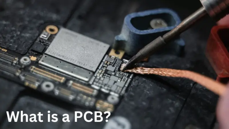
What is a PCB?
PCBs come in different sizes and complexities, depending on the specific application and requirements of the electronic device. They can range from simple single-layer boards used in basic consumer electronics to complex multi-layer boards used in advanced computing systems. The advantages of using PCBs in electronic devices are numerous. They provide a compact and organized layout for components, reducing the overall size of the device. PCBs also offer improved reliability and durability, as the connections between components are more stable compared to manual wiring. Additionally, PCBs allow for easier troubleshooting and repair, as faulty components can be easily identified and replaced.
Get Instant Online Quote
Board Class
The Board Class is a classification system used to categorize the quality and reliability of a printed circuit board. It helps manufacturers and designers to understand the capabilities and limitations of a PCB, ensuring that it meets the specific requirements of a particular application. The Board Class is determined by various factors, including the materials used, the fabrication processes employed, and the level of testing and inspection performed. These factors collectively determine the overall quality and performance of the PCB. There are several different Board Classes, each with its own set of requirements and specifications. The most common classes are Class 1, Class 2, and Class 3.
>Reference: IPC 6012 Guidelines: Classifying, Designing, and Fabricating PCBs
Class 1: Class 1 PCBs are typically used in consumer electronics and other low-cost applications where functionality is the primary concern. These boards have the lowest requirements in terms of performance and reliability. They are often single-sided or double-sided boards with simple designs and limited functionality.
Class 2: Class 2 PCBs are used in a wide range of applications, including automotive, industrial, and telecommunications. They have higher requirements in terms of performance and reliability compared to Class 1 boards. Class 2 boards are typically multi-layered with more complex designs and functionality.
Class 3: Class 3 PCBs are the highest quality and most stringent boards. They are used in critical applications such as aerospace, military, and medical devices, where reliability is of utmost importance. Class 3 boards undergo extensive testing and inspection to ensure they meet the highest standards of performance and reliability.
> Recommend reading: IPC Class 2 vs 3: The Differences in PCB IPC Standards
Types of Printed Circuit Board
Printed Circuit Boards (PCBs) are an essential component of electronic devices. They provide a platform for connecting and supporting various electronic components, making them an integral part of modern technology. PCBs come in different types, each designed for specific applications and requirements. We will explore the different types of printed circuit boards and their uses.
Single-Layer/Sided PCBs: Single-sided PCBs are the simplest and most basic type of PCB. They consist of a single layer of substrate material, usually made of fiberglass or phenolic resin, with a thin layer of copper on one side. The copper layer is etched to create the desired circuit pattern. Single-layer PCBs are commonly used in simple electronic devices with fewer components and simpler circuitry.
2 Layer/Double-Layer PCBs: 2 Layer PCBs have copper layers on both sides of the substrate material. The circuitry is created by etching the desired pattern on both sides, and the two layers are connected using plated through-holes. Double-sided PCBs provide more space for components and allow for more complex circuit designs. They are widely used in a variety of applications, from consumer electronics to industrial equipment.
Multi-Layer PCBs: Multi-layer PCBs consist of multiple layers of substrate material with copper layers in between. The number of layers can vary, ranging from four to sixteen or more, depending on the complexity of the circuit design. The layers are connected using plated through-holes, providing a high level of connectivity and allowing for more intricate circuitry. Multi-layer PCBs are commonly used in high-end electronic devices, such as smartphones, computers, and advanced medical equipment.
Rigid PCBs: Rigid PCBs are the most common type of PCB and are made from rigid materials such as fiberglass or epoxy. They provide a solid and durable platform for electronic components and are widely used in various industries. Rigid PCBs are known for their stability and reliability, making them suitable for applications where the circuitry needs to remain fixed and secure.
Flexible PCBs: Flexible PCBs, also known as Flex PCBs, are made from flexible materials such as polyimide. They offer the advantage of being able to bend and twist, making them ideal for applications where space is limited or where the circuitry needs to conform to a specific shape. Flexible PCBs are commonly used in wearable devices, automotive electronics, and aerospace applications.
Rigid-Flex PCBs: Rigid-Flex PCBs combine the advantages of both rigid and flexible PCBs. They consist of rigid sections and flexible sections, allowing for complex circuit designs that can be folded or bent. Rigid-Flex PCBs are used in applications where durability, space-saving, and flexibility are required, such as in military equipment, robotics, and high-end electronic devices.
The Process of Printed Circuit Board Design
Printed Circuit Board (PCB) design is like creating a blueprint that outlines the layout and connections of components on a circuit board. This process ensures that the final product functions as intended and meets the necessary specifications. The first step in PCB design is to gather the requirements and specifications for the circuit board. This includes determining the size, shape, and number of layers required, as well as the types of components that will be used. Once these requirements are established, the designer can move on to the next step.
The next stage involves creating a schematic diagram, which is a visual representation of the circuit. This diagram shows how the components are connected and allows the designer to identify any potential issues or conflicts. It is an essential tool for ensuring the functionality and efficiency of the circuit. After the schematic is complete, the designer moves on to the layout phase. This involves placing the components on the circuit board and routing the connections between them.
The goal is to create a layout that minimizes signal interference and maximizes efficiency. Once the layout is finalized, the designer generates the manufacturing files. These files contain all the necessary information for producing the circuit board, including the component placement, routing, and drill holes. To ensure the highest quality and reliability in PCB production, designers often follow industry standards like IPC-J-STD-001& IPC-A-610 Standard, which defines requirements for soldered electrical and electronic assemblies.The files are then sent to a manufacturer like NextPCB, who produces the PCB according to the specifications.
DFM/DFA
What is DFM/DFA? - Design for Manufacturability (DFM) is the process of designing a PCB in such a way that it can be easily and cost-effectively manufactured. DFM focuses on identifying and eliminating potential manufacturing issues early in the design stage, reducing the risk of costly rework or delays during production. DFM encompasses various design considerations, including component placement, routing, and material selection. Design for Assembly (DFA) is a complementary concept to DFM, focusing specifically on optimizing the assembly process. DFA aims to simplify and streamline the assembly of the PCB by reducing the number of assembly steps, minimizing the risk of errors, and enhancing overall productivity.
- > Recommend reading: DFM, DFMA, DFA. Part 1. Kicad and Online Gerber Viewer
- > Recommend reading: DFM, DFMA, DFA. Part 2. NextPCB's PC program
Next PCB integrates advanced tools and methodologies into their platform to ensure optimal manufacturability, covering both DFM and DFA capabilities:
- Automated DFM Checks: NextPCB HQDFM performs automated checks during the design process to identify potential manufacturing issues. These checks include clearance violations, solder mask errors, and component placement constraints. By detecting and flagging these issues early on, designers can make necessary adjustments to improve manufacturability.
- Real-time Feedback: NextPCB HQDFM provides real-time feedback on design choices that may affect manufacturability. This includes suggestions on trace widths, pad sizes, and component footprints. By leveraging their expertise and industry knowledge, Next PCB ensures that designs meet manufacturing requirements without compromising functionality.
- Design Rule Check (DRC): NextPCB HQDFM DRC feature verifies designs against a comprehensive set of manufacturing rules. This ensures that the design adheres to industry standards and best practices, minimizing the risk of manufacturing issues. The DRC feature also allows designers to customize manufacturing rules based on specific requirements.
- Component Placement Optimization: NextPCB HQDFM provides automated component placement optimization, ensuring that components are positioned in a way that minimizes assembly time and reduces the chances of errors. By optimizing component placement, Next PCB improves overall assembly efficiency.
- Assembly-Friendly Design Guidelines: NextPCB HQDFM offers comprehensive design guidelines that facilitate assembly-friendly PCB layouts. These guidelines cover aspects such as component spacing, orientation, and labeling, ensuring that the PCB design is easy to assemble and reduces the risk of misplacement or soldering errors. > You may want to take a reference: PCB Assembly - The Most Comprehensive Guide | NextPCB
- Design for Test (DFT): NextPCB HQDFM supports Design for Test (DFT) methodologies, which involve designing PCBs in a way that simplifies the testing process. By incorporating DFT principles, Next PCB ensures that the assembly and testing phases are seamless, resulting in improved product quality and faster time-to-market.
> See Practical DFM Checklist and HQDFM Practice
Try HQDFM For Free
How to Make a Printed Circuit Board
Printed Circuit Boards (PCBs) are essential components in modern electronic devices. They provide a platform for connecting and supporting various electronic components, allowing them to function together seamlessly. Creating your own PCB may seem like a difficult task, but with the right tools and knowledge, it can be a rewarding and cost-effective endeavor.
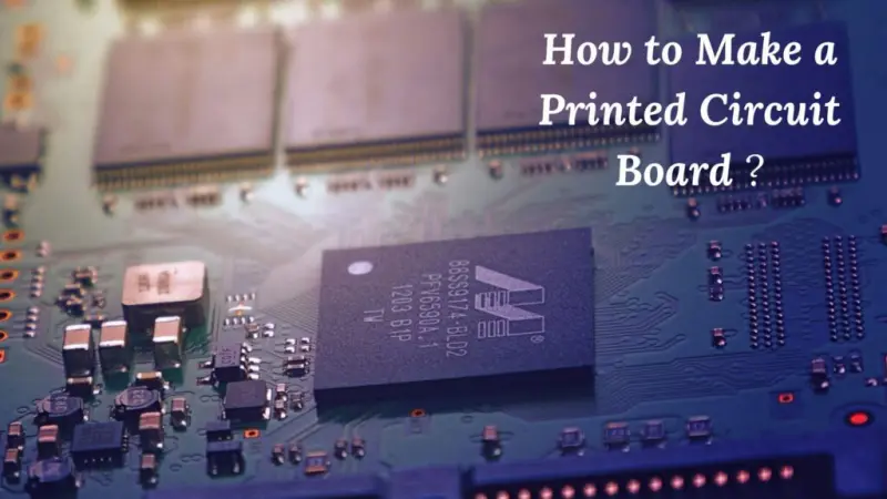
How to Make a Printed Circuit Board
Create the Schematic
When it comes to designing a printed circuit board (PCB), one of the first steps is creating the schematic. The schematic is a visual representation of the circuit that shows how the components are connected and how they interact with each other. It serves as a blueprint for the PCB layout and is important for ensuring that the final board functions as intended. The schematic consists of various symbols that represent different electronic components such as resistors, capacitors, transistors, and integrated circuits. These symbols are interconnected by lines that indicate the electrical connections between the components.
To create the schematic, you'll need the right software. There are several options available, both free and paid, that provide a user-friendly interface and a wide range of features. Some popular choices include Eagle, Altium Designer, KiCad, and OrCAD. Consider your specific requirements, budget, and level of expertise when selecting the software that best suits your needs. Once you have chosen the software, familiarize yourself with its interface and tools. Most software packages offer libraries of pre-designed components that you can use in your schematic. These libraries save time and ensure accuracy by providing standardized symbols and footprints for commonly used components.
Simulate the Circuitry
Once the schematic sets the stage, the next step in the journey of creating a Printed Circuit Board (PCB) is to simulate the circuitry. Simulating the circuitry in a PCB offers several benefits. It allows engineers to verify the functionality of the circuit before investing time and resources in pcb manufacturing. By identifying and rectifying any design flaws or errors in the simulation stage, costly mistakes can be avoided. Simulations also help in optimizing the circuit's performance, ensuring that it meets the desired specifications. Furthermore, simulating the circuitry provides insights into the behavior of the circuit under different conditions. It helps in understanding how the circuit will respond to changes in voltage, current, temperature, and other factors. This information is valuable for troubleshooting and fine-tuning the circuit design.
There are various tools and techniques available for simulating circuitry in a PCB. Here are some commonly used ones:
1. SPICE (Simulation Program with Integrated Circuit Emphasis): SPICE is a widely used circuit simulation program that allows engineers to analyze and predict the behavior of electronic circuits. It uses mathematical models to simulate the performance of components such as resistors, capacitors, transistors, and integrated circuits. SPICE provides accurate results and is capable of simulating both analog and digital circuits.
2. Breadboarding: Breadboarding is a technique where the circuit is built on a breadboard using actual electronic components. It allows for quick prototyping and testing of the circuit. While breadboarding does not provide the same level of accuracy as software simulations, it can be useful for simple circuits or when physical testing is required.
3. Virtual Prototyping: Virtual prototyping involves creating a digital model of the PCB and simulating its behavior using specialized software. This approach allows for a more comprehensive analysis of the circuit, taking into account factors such as signal integrity, power distribution, and thermal management. Virtual prototyping enables engineers to optimize the PCB design for performance, reliability, and manufacturability. > Recommend reading: Fundamentals of PCB Thermal Design | NextPCB
4. Signal Integrity Analysis: Signal integrity analysis is a crucial aspect of PCB simulation, especially for high-speed digital circuits. It involves analyzing the quality of signals in terms of their timing, voltage levels, and noise. By simulating the signal integrity, engineers can identify and mitigate issues such as signal reflections, crosstalk, and electromagnetic interference.
CAD Tool Setup
To design and create PCBs, engineers and designers rely on Computer-Aided Design (CAD) tools. Before diving into the setup process, it's important to choose the right CAD tool for your PCB design needs. There are several CAD tools available in the market, each with its own set of features and capabilities. Some popular options include Altium Designer, Eagle, KiCad, and OrCAD. Consider factors such as ease of use, compatibility with your operating system, and the specific features you require for your PCB design projects. Once you have selected a CAD tool, it's crucial to ensure that your computer meets the necessary system requirements. CAD tools can be resource-intensive, so it's important to have a computer with sufficient processing power and memory. Check the software's official documentation or website for the specific system requirements. Ensure that your computer meets or exceeds these requirements to avoid any performance issues during the design process.
After installing the CAD tool, it's time to configure and customize it according to your preferences. Most CAD tools offer a range of customization options to tailor the software to your specific needs. Some common configuration settings include:
- Units of measurement: Choose between metric or imperial units.
- Grid settings: Adjust the grid size and spacing for precise placement of components.
- Shortcuts and hotkeys: Customize keyboard shortcuts for faster workflow.
- Default libraries: Set up default component libraries for quick access.
- Design rules: Define specific design rules for your PCB projects.
Once you have set up your CAD tool, it's important to familiarize yourself with its features and functionalities. Most CAD tools offer comprehensive documentation and tutorials to help you get started. Take advantage of these resources to learn the ins and outs of the software. Additionally, online communities and forums can be valuable sources of support and knowledge. Engage with fellow PCB designers, ask questions, and share your experiences to enhance your skills and troubleshoot any issues you may encounter.
Place Components
Component placement is more than just arranging parts on a PCB. It directly affects the electrical performance, signal integrity, and manufacturability of the final product. Proper component placement ensures that signals can flow efficiently between components without interference or degradation. By minimizing the length of signal traces and reducing the number of vias, designers can improve signal integrity and reduce the risk of noise or signal loss.
Components generate heat during operation, and effective component placement is essential for proper thermal management. By considering heat-generating components and their proximity to heat sinks or cooling mechanisms, designers can prevent overheating and ensure the longevity of the device. Efficient component placement can streamline the manufacturing process. By grouping components logically and considering the accessibility for soldering and testing, manufacturers can reduce assembly time and minimize the risk of errors or rework.
> Expand reading: Circuit Board Solder: Types, Temperatures & How to Choose (Reflow & Hand Soldering Tips)
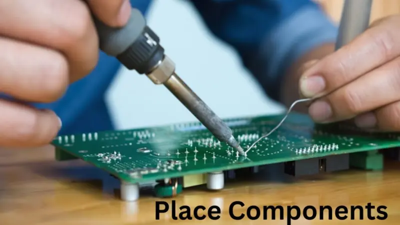
Place Components on PCB
Route the PCB
Routing refers to the process of creating connections between different components on the PCB, ensuring that the electrical signals flow smoothly and efficiently. It determines the overall performance, reliability, and manufacturability of the circuit board. Proper PCB routing helps to minimize signal interference, reduce noise, and optimize the flow of electrical signals. It also ensures that the PCB meets the required electrical and mechanical specifications. Before you start routing, it is essential to have a clear plan for your PCB layout. Consider the placement of components, the size of the board, and any specific design requirements. To minimize signal interference, it is important to separate different signal types. Group similar signals together and keep high-speed signals away from sensitive analog or low-speed signals. This will help to reduce crosstalk and ensure better signal integrity. The width of the traces and the spacing between them are critical for maintaining the required impedance and preventing signal degradation. Consult the design guidelines provided by your PCB manufacturer to determine the appropriate trace widths and spacing for your design. Vias are used to connect different layers of the PCB. While they are necessary, excessive use of vias can increase the complexity of the design and affect signal integrity. Minimize the number of vias and keep them away from high-speed signal paths to reduce signal reflections and losses.
Ensure a Clear PCB Return Current Path
When designing a printed circuit board (PCB), one of the critical factors to consider is the return current path. The return current path refers to the path that the current takes to complete the circuit and return to its source. A clear and well-defined return current path is essential for the proper functioning of the PCB and to avoid any potential issues.
- Signal Integrity: A well-defined return path helps maintain signal integrity by minimizing noise and interference. It ensures that the return current flows in close proximity to the signal current, reducing the chances of signal degradation.
- EMI/EMC Compliance: A clear return current path helps in meeting electromagnetic interference (EMI) and electromagnetic compatibility (EMC) requirements. It reduces the chances of unintentional radiation and susceptibility to external noise sources.
- Power Distribution: In power distribution systems, a clear return current path is essential to ensure efficient power delivery and minimize voltage drops. It helps prevent ground loops and ensures proper functioning of the circuit.
Final Rules Check
The final rules check is important because it helps to identify any potential issues or errors in the PCB design before it goes into production. By conducting a thorough check, you can catch and rectify any design flaws, manufacturing inconsistencies, or assembly errors that could affect the performance and reliability of the PCB. Here are some key areas that are typically reviewed during the final rules check:
Design Rule Check (DRC): The Design Rule Check is an essential part of the final rules check process. It involves verifying the design against a set of predefined rules that ensure the board's manufacturability and functionality. The DRC checks for issues such as trace width violations, spacing violations, and other design rule violations that could impact the performance of the PCB.
Manufacturing Rules Check: The manufacturing rules check focuses on reviewing the design for any manufacturing-related issues. This includes checking for proper clearances, component footprints, solder mask openings, and other manufacturing constraints. By ensuring that the design adheres to the manufacturing rules, you can minimize the risk of production delays or costly rework.
Component Placement and Footprint Check: During the final rules check, it is important to review the component placement and footprints on the PCB. This involves verifying that the components are correctly placed and aligned with the corresponding footprints on the board. Any discrepancies or errors in component placement can lead to electrical or mechanical issues.
Signal Integrity Check: The signal integrity check is crucial for ensuring that the electrical signals on the PCB are transmitted without any distortions or losses. This involves analyzing the signal paths, trace lengths, impedance matching, and other factors that can impact signal integrity. By conducting a thorough signal integrity check, you can optimize the performance and reliability of the PCB.
Assembly Rules Check: The assembly rules check focuses on reviewing the design for any issues that could affect the assembly process. This includes checking for proper component orientation, polarity, and solderability. By ensuring that the design complies with the assembly rules, you can minimize the risk of assembly errors and improve the overall quality of the finished PCB.
PCB Manufacturing and Assembly
The PCB manufacturing process involves several steps, each of which is crucial in ensuring the production of high-quality and reliable PCBs. Let's explore each step in detail:
- Designing the PCB: The first step in PCB manufacturing is designing the circuit board. This involves creating a schematic diagram using computer-aided design (CAD) software. The schematic diagram outlines the connections between various components and serves as a blueprint for the PCB layout.
- PCB Prototyping: Once the PCB design is complete, a prototype is created to test its functionality. Prototyping helps identify any design flaws or errors before moving on to mass production. It allows for adjustments and refinements to be made to ensure optimal performance.
- PCB Fabrication: After the prototype has been approved, the PCB fabrication process begins. This involves transferring the PCB design onto a laminate material, typically made of fiberglass or composite epoxy. The design is etched onto the laminate using a chemical process, creating the copper traces and pads that form the circuitry.
- Component Sourcing: Once the PCBs are fabricated, the next step is sourcing the electronic components that will be mounted on the board. This includes resistors, capacitors, integrated circuits, connectors, and more. It is essential to source high-quality components from reliable suppliers to ensure the overall reliability and performance of the PCB.
The PCB assembly process involves mounting the sourced components onto the fabricated PCB. There are two main methods of PCB assembly:
- Through-Hole Assembly: In this method, the components are inserted into pre-drilled holes on the PCB and soldered onto the copper pads on the opposite side.
- Surface Mount Assembly: This method involves soldering the components directly onto the surface of the PCB. Surface mount components are smaller and lighter, allowing for more compact and efficient designs.
> Expand reading: PCB Assembly - The Most Comprehensive Guide | NextPCB
> Expand reading: PCB/PCBA Test Methods by Category
> Expand reading: The Core of System Integration: Box Build Assembly in Electronics Manufacturing
Get Free PCB Assembly
Conclusion
In conclusion, understanding the basics of printed circuit board (PCB) design is essential for anyone involved in electronics or engineering. From the initial concept to the final artwork, each step in the process plays an important role in ensuring a functional and efficient PCB.
It is important to consider the board class and choose the appropriate type of PCB based on the specific requirements of the project. The process of PCB design involves several stages, including design for manufacturing (DFM) and design for assembly (DFA).
These steps help optimize the design for efficient production and assembly. Creating a PCB involves tasks such as creating the schematic, simulating the circuitry, setting up the CAD tool, placing components, and routing the PCB.
Once the design is finalized, PCB manufacturing and assembly take place. This involves the fabrication of the PCB and the placement of components onto the board. Remember, the world of PCB design is constantly evolving, and it's important to stay updated with the latest advancements and best practices. With NextPCB, you can create high-quality PCBs that meet your project's requirements.
Request an Online Quote for Your Next PCB
About the Author
Julia Wu - Senior Sales Engineer at NextPCB.com
With over 10 years of experience in the PCB industry, Julia has developed a strong technical and sales expertise. As a technical sales professional, she specializes in understanding customer needs and delivering tailored PCB solutions that drive efficiency and innovation. Julia works closely with both engineering teams and clients to ensure high-quality product development and seamless communication, helping businesses navigate the complexities of PCB design and manufacturing. Julia is dedicated to offering exceptional service and building lasting relationships in the electronics sector, ensuring that each project exceeds customer expectations.


 NextPCB Capabilities
 PCB Assembly
 Layer Buildup
 SMD-Stencils
 PCB Design-Aid & Layout
 Mechanics
 Surface
 Quality
 Drills & Throughplating
 Factory & Certificate


