PCB Silkscreen Printing Specifications
- 1. All components, mounting holes, and positioning holes have corresponding silkscreen labels. In order to facilitate the installation of fabricated boards, all components, mounting holes, and positioning holes have corresponding silkscreen labels. The silkscreen of mounting holes on PCB is marked with H1, H2... HN.
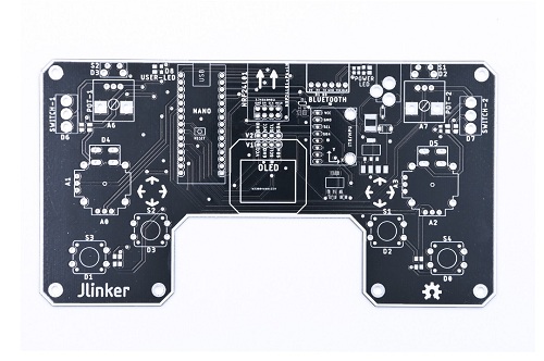
- 2. The PCB silkscreen characters shall follow the principle of from left to right and from bottom to top. The silkscreen characters shall follow the principle of from left to right and from bottom to top as far as possible. For devices with polarity such as electrolytic capacitors and diodes, the direction shall be consistent in each functional unit as far as possible.
- 3. There is no PCB silkscreen on the device pad and tin channel to be tinned, and the device tag number shall not be blocked by the device after installation( High density, except those that do not need silk-screen printing on PCB). In order to ensure the welding reliability of the device, it is required that there is no silkscreen on the device pad; In order to ensure the continuity of tin lined raceways, it is required that there is no silkscreen on the tin-lined raceways; In order to facilitate device insertion and maintenance, the device tag number shall not be obscured by the device after installation; The PCB silkscreen shall not be pressed on the through-hole and pad, so as to avoid losing part of the silkscreen when opening the resistance welding window and affecting the identification. The screen printing spacing is greater than 5MIL.
- 4. The polarity of components with polarity is clearly indicated on the PCB silkscreen, and the polarity direction mark is easy to identify.
- 5. For connectors with direction, the direction shall be clearly indicated on the silkscreen.
- 6. The PCB shall be provided with bar code position identification. When the PCB surface space allows, the PCB shall be provided with 42 * 6mm bar code silkscreen frame, and the position of the bar code shall be convenient for scanning.
- 7. The name, date, version number, and other information of the PCB board shall be clearly located. The PCB file shall have the board name, date, version number, and other board information silk screen printing, with a clear and eye-catching position.
- 8. The PCB shall have complete relevant information and anti-static identification of the manufacturer.
- 9. The number of PCB photo files is correct. Each layer should have correct output and complete layer output.
- 10. The identifier of the device on the PCB must be consistent with the identification symbol in the BOM.
Considerations for designing printouts of PCB silkscreen
- 1. The layers to be output are:
(1) The wiring layer includes top layer/bottom layer / intermediate wiring layer/power supply layer, including VCC layer and GND layer;
(2) the screen printing layer includes top screen printing/bottom screen printing/
(3) the solder resist layer includes top layer solder resist and bottom layer solder resist
(4) Ncdrill also generates a drilling file
- 2. If the power layer is set to split / mixed, select routing in the document item of the add document window, and use the plane connect of pour manager to copper the PCB diagram before outputting the photo file every time; If it is set to complain, select plane. When setting the layer item, add layer25 and select pads and vias in layer25.
- 3. In the device setting window, press device setup to change the value of aperture to 199
- 4. Select board outline when setting the layer of each layer
- 5. When setting the layer of the PCB silkscreen layer, do not select the part type, and select the outline text line of the top layer, bottom layer, and silkscreen layer.
- 6. When setting the layer of solder resist layer, selecting via means no solder resist is added to the via, and selecting no via means solder resist is determined according to the specific situation.
- 7. When generating drilling files, use the default settings of PowerPC and do not make any changes
- 8. After all photo files are output, open them with CAM350 and print them. The designer and reviewer shall check them according to the "PCB Checklist".
PCB QUOTE
Safety regulations and identification requirements
- 1. The safety regulation marks of the fuse tube are complete, and whether there are 6 complete marks near the fuse, including fuse serial number, fusing characteristics, rated current value, explosion-proof characteristics, rated voltage value, and English warning marks. For example, F101, f3.15ah, 250VAC, " Caution: for continued protection against the risk of fire, replace only with the same type and rating of fuse". If there is no space to arrange English warning signs on the PCB, the English warning signs can be placed in the product manual.
- 2. The hazardous voltage area on the PCB shall be marked with a high voltage warning sign. The hazardous voltage area of the PCB shall be isolated from the safe voltage area with a 40mil wide dotted line, and printed with a high voltage hazard sign and "danger! HIGH VOLTAGE ”.
- 3. The primary and secondary isolation strips are clearly marked, and the primary and secondary isolation strips of PCB are clearly marked with dotted lines in the middle.
- 4. PCB safety regulations and marks shall be clear and complete. DANGER!!! HIGH VOLTAGE

 NextPCB Capabilities
 PCB Assembly
 Layer Buildup
 SMD-Stencils
 PCB Design-Aid & Layout
 Mechanics
 Quality
 Drills & Throughplating
 Factory & Certificate
 PCB Assembly Factory Show
Certificate
PCB Assembly Factory Show
Certificate


 Surface

