
 NextPCB Capabilities
Printed Circuit Boards
NextPCB Capabilities
Printed Circuit Boards
 PCB Assembly
 Layer Buildup
 SMD-Stencils
 PCB Design-Aid & Layout
 Mechanics
 Quality
 Drills & Throughplating
 Factory & Certificate
 PCB Assembly Factory Show
Certificate
PCB Assembly Factory Show
Certificate
Support Team
Feedback:
support@nextpcb.com


Electromagnetic interference or EMI originates from electromagnetic radiation and refers to any form of background noise or disturbance that possibly traces back to it. Electronic devices and machinery may experience performance degradation or improper functioning as a result of this interference. Radio waves, other electronics' radiated EM fields, power supply oscillations, and mechanical systems' radiated EM fields are all potential causes of EMI.
In contrast, EMC (Electromagnetic Compatibility) describes how well electronic devices and equipment function when exposed to electromagnetic interference. Performing electromagnetic compatibility (EMC) testing is necessary. To prevent electromagnetic interference (EMI) from disrupting the operation of any electronic device or piece of equipment.
PCB designers frequently use EMI and EMC together in the layout process. Making a circuit that is both EMI-proof and compatible with other electronics in use nearby is a top priority for designers. The device's ability to resist electromagnetic interference (EMI) from other sources and operate successfully depends on the quality of the executed EMC design.
Designing for electromagnetic interference and electromagnetic compatibility involves a few considerations, like the nature of the transmitted signals, the circuit's layout, and the materials. Careful grounding, shielding, and filtering procedures can lessen EMI's effect on the PCB, while strategically placed components can boost EMC.
In this article,
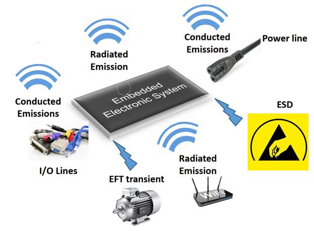
There are many potential environmental causes of EMI (Electromagnetic Interference). They may come from places like:
PCB designers need to think about the various possible ambient sources of electromagnetic interference (EMI) when making electrical gadgets. Using the appropriate shielding, filtering, and grounding techniques can protect the dependable operation of electronic circuits against EMI.
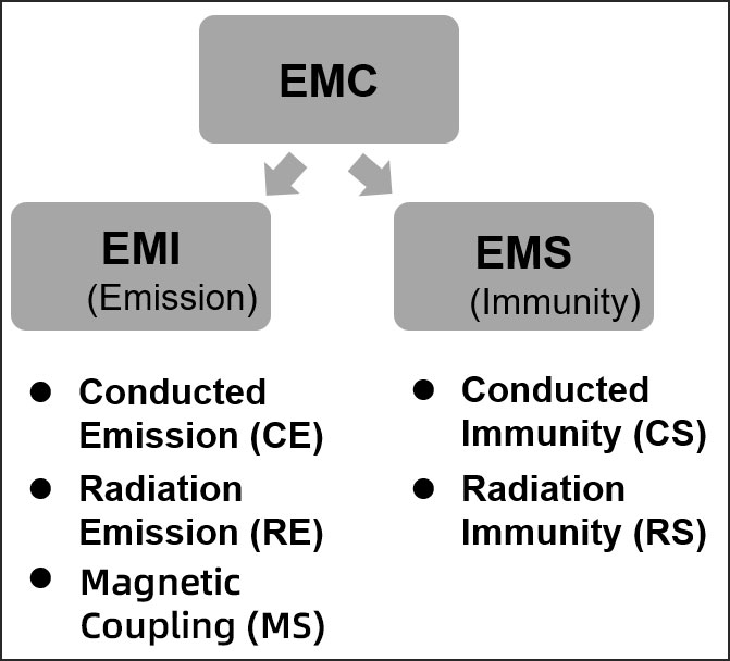
Electromagnetic Interference can impair the performance and functionality of a PCB in several ways. Conducted and radiated EMI are the two most common types of electromagnetic interference.
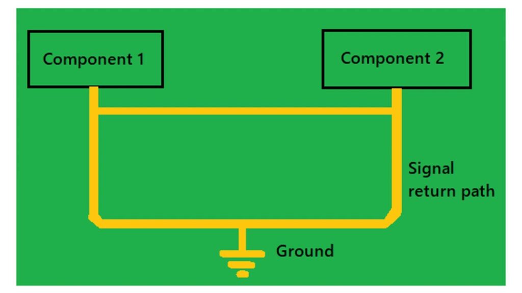
The term "conducted EMI" refers to electromagnetic interference that travels along the conductors of a PCB. The power supply can also cause conducted EMI by introducing noise and ripple onto the power rails of a PCB. PCB designers can mitigate conducted EMI through filters, ferrite beads, and suitable grounding techniques.
In contrast, radiated EMI is the form of EMI that travels over space as electromagnetic waves. Radiated electromagnetic interference can be a severe worry for PCB designers, as it can interact with surrounding equipment and systems. To prevent radiated EMI, PCB designers can utilize shielding, grounding, and careful PCB layout design.
Magnetic coupling is another type of EMI that happens. Happen when the magnetic field produced by one circuit causes a voltage in a nearby circuit. Magnetic coupling can be problematic for analog low-level circuits that are sensitive to slight voltage fluctuations. PCB designers can utilize shielding, spacing, and twisted pair wire to reduce magnetic coupling.
There are various types of electromagnetic interference that can affect the performance and operation of a PCB. Radiated EMI propagates through space as electromagnetic waves, while magnetic coupling occurs when the magnetic field generated by one circuit induces a voltage in a nearby circuit. To achieve EMC compliance with their designs, PCB designers must account for different types of EMI and employ the proper mitigation strategies.
EMI can have a substantial effect on the performance and dependability of a PCB. Therefore, it is essential to employ the proper mitigation measures to limit the impacts of EMI on the PCB. Here are four common EMI mitigation techniques:
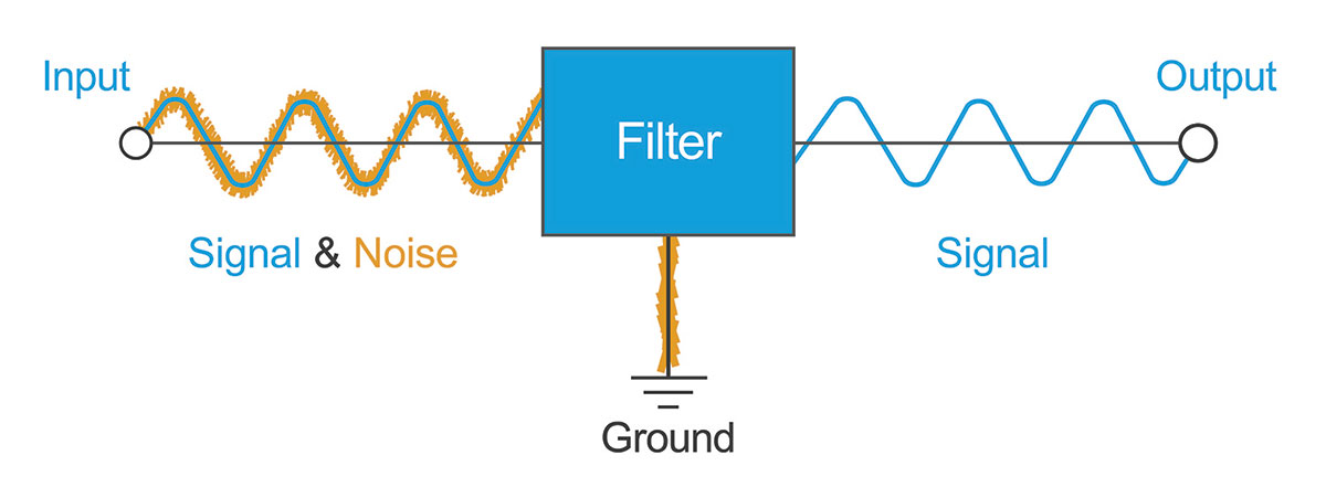
EMI can have a substantial effect on a PCB's performance and dependability. Employing proper mitigation techniques such as shielding, grounding, filtering, and careful PCB layout design can help to decrease the impacts of EMI and ensure that the PCB is EMC compliant.
Making sure electrical devices can function without causing or being damaged by electromagnetic interference (EMI) is important in PCB design. The EMC testing standards that PCB designers must be familiar with vary from one market to the next.
The United States Federal Communications Commission (FCC) provides one of the most extensively used benchmarks for EMC testing. The Federal Communications Commission (FCC) establishes guidelines for acceptable levels of radiated and conducted emissions from electronic devices and mandates that all such devices be tested and certified for compliance. As wireless devices, like cell phones and Wi-Fi routers, might interfere with others operating in the same frequency range, this is especially crucial for them.
The CE marking established by the European Union is another significant standard. Products marketed in the European Union (EU) must bear the CE label, which certifies that they meet EU health, safety, and environmental regulations. Electromagnetic compatibility (EMC) testing is part of the CE certification process, and the standard specifies the allowable ranges for emissions (radiated and conducted) and susceptibility (to electromagnetic fields).
VCCI in Japan, ICES in Canada, and CISPR in Europe are a few examples of countries that have their own EMC testing standards. Radiated and conducted emissions, as well as tolerance to electromagnetic fields, are common areas of overlap between these standards.
Emissions and immunity testing are common components of EMC analysis. Testing for emissions ensures that the device does not produce excessive electromagnetic radiation that could disrupt other electronics while testing for immunity verifies that the gadget continues to function normally even when subjected to external electromagnetic fields.
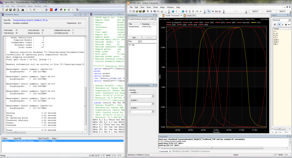
Tools for electromagnetic interference simulation play a crucial role in designing and developing printed circuit boards. These programs aid in the analysis and forecasting of EMI problems that a PCB may encounter, allowing designers to better prepare for them.
A variety of electromagnetic interference simulation tools, such as SPICE (Simulation Program with Integrated Circuit Emphasis), are at your disposal. SPICE is widely used to describe the electrical properties of PCBs and simulate the behavior of electronic circuits. On the other hand, PCB components and their interactions with electromagnetic fields can be modeled with electromagnetic simulation software.
The ability to spot EMI problems early on in the design process is a major advantage of EMI simulation tools. This can cut down on the price tag and time spent on building and testing physical prototypes. Instead of building physical prototypes first, designers might utilize simulation tools to test and iterate on potential designs.
PCB layouts can be optimized for EMI performance with the aid of simulation tools, which can be used by designers. You can use them to simulate how various component positions, trace routing alternatives, and grounding methods will affect EMI performance. This helps designers find the optimal arrangement for their project and prevent EMI problems.
PCB design and development are incomplete without EMI simulation tools. They help designers spot and correct EMI problems early on, optimize their layouts for optimum EMI performance, and guarantee that their PCBs are in compliance with all applicable EMC (Electromagnetic Compatibility) regulations.
Making sure electronic equipment doesn't generate or isn't affected by electromagnetic interference (EMI) is dependent on careful PCB design for EMC. While designing for electromagnetic compatibility, PCB designers should bear the following in mind:
PCB designers must pay great attention to component selection, PCB layout, power supply design, shielding, filtering, and testing to ensure their boards comply with electromagnetic compatibility (EMC) standards.
In conclusion, RF interference and electromagnetic compatibility are fundamental principles for any PCB designer to grasp. Electromagnetic interference (EMI) is a major contributor to the malfunction, noise, and decreased performance of electronic devices. Yet, EMC ensures that all electrical components may work together in harmony regardless of the presence or absence of electromagnetic fields.
PCB layout, component choice, grounding, and shielding are all factors that must be taken into account while designing for electromagnetic compatibility. Filtering, shielding, and grounding are just some of the methods that might help designers reduce EMI. To further guarantee that their PCBs are in accordance with all applicable regulations, designers must follow many EMC testing standards.
The significance of EMC and EMI mitigation will increase in the next years as the technology in use increases. To ensure their devices conform to rigorous standards and function as intended, PCB designers must stay abreast of evolving EMC legislation and industry best practices.
Ultimately, the success of electronic products and gadgets depends on a thorough comprehension of EMI and EMC. It is possible for designers to make EMC-compliant and dependably functioning PCBs by adhering to best practices, making use of simulation tools, and doing extensive testing.
Still, need help? Contact Us: support@nextpcb.com
Need a PCB or PCBA quote? Quote now


 Surface

