
 Surface


Arya Li, Project Manager at NextPCB.com

 NextPCB Capabilities
Printed Circuit Boards
NextPCB Capabilities
Printed Circuit Boards
 PCB Assembly
 Layer Buildup
 SMD-Stencils
 PCB Design-Aid & Layout
 Mechanics
 Quality
 Drills & Throughplating
 Factory & Certificate
 PCB Assembly Factory Show
Certificate
PCB Assembly Factory Show
Certificate
Support Team
Feedback:
support@nextpcb.com


Introduction
In the highly specialized arena of modern electronics manufacturing, the speed and accuracy of Printed Circuit Board assembly (pcba) have reached an astonishing micrometer scale. Driving this automated revolution are the seemingly trivial circular copper dots known as Fiducial Marks. They function as the optical anchor points for machine vision systems, serving as the silent language that ensures billions of components are placed with impeccable precision.
For PCB engineers and designers, understanding and strictly implementing industry standards for fiducial marks is a critical step toward transitioning successfully from prototyping to mass production. An incorrectly designed fiducial can halt an entire SMT line or cause catastrophic yield loss during high-volume manufacturing. Especially when dealing with fine-pitch components, complex double-sided assemblies, and dimensionally unstable flexible PCBs, the quality and layout of fiducial marks are a lifeline for product reliability.
This article, written from the perspective of a seasoned industry expert, provides an in-depth analysis of the core function and highest standards of practice for fiducial marks. We will go beyond the basic IPC/SMEMA guidelines to discuss how the three-point positioning system compensates for non-linear geometric distortion, how to select the optimal surface finish (such as ENIG or Immersion Tin) to meet the demanding requirements of 3D Solder Paste Inspection (SPI), and the advanced strategies mandatory for High-Reliability (IPC Class 3) and flexible circuit designs. This guide is intended to provide a comprehensive, practical resource for all professionals focused on electronics quality and manufacturing efficiency.
Table of Contents
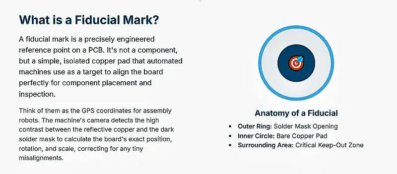
Fiducial Marks, often referred to in the PCB industry as “target points” or “optical alignment marks,” are precisely engineered geometric features that serve as reliable reference points for high-speed, high-precision automated assembly processes. These markers allow machine vision systems across the Surface Mount Technology (SMT) production line to accurately determine the board's absolute position and orientation, and compensate for geometric deviations incurred during the manufacturing process.
Every critical step, from stencil printing (Solder Paste Inspection, SPI) to component placement (Pick-and-Place), relies on fiducial marks as common, measurable reference points. A well-designed fiducial enables the machine to calculate the PCB's displacement in the X/Y axes and its rotation (θ) relative to the preset assembly path.
To guarantee placement accuracy, fiducial marks must be physically created as part of the circuit pattern (Copper Artwork) and etched during the same process step as the SMT pads. This co-manufacturing ensures the highest possible relative positional accuracy between the fiducial and the SMT pads. Using screen-printed features or drill holes as alignment references is unacceptable because they are added in separate processes, resulting in lower registration accuracy that compromises final component placement precision.
Modern electronics assembly faces challenges beyond simple two-dimensional (2D) positioning. PCBs, especially large panels or thin boards made of composite materials like FR-4, undergo unavoidable expansion, contraction, and mechanical stress when exposed to high temperatures during reflow soldering. This thermal stress can cause subtle geometric deformations such as warp, twist, or non-linear stretch and shrinkage.
If the assembly machine relies only on simple X/Y/θ translational and rotational correction, it cannot accurately match the true location of pads far from the center, especially for fine-pitch components (e.g., BGAs, QFNs). This leads to significant placement error and reduced yield. Therefore, the core value of a fiducial system is its ability to allow the machine vision system to identify at least three points to calculate a complex mathematical compensation matrix (typically an Affine Transformation). This matrix is used to correct these local and global non-linear distortions in real-time. This planar distortion compensation capability is essential for achieving high-precision, high-yield automated assembly.
To ensure interoperability and high recognition rates across different SMT equipment (e.g., printers, placement machines), fiducial mark design must strictly adhere to industry standards, notably those set by IPC (Association Connecting Electronics Industries) and SMEMA (Surface Mount Equipment Manufacturers Association).
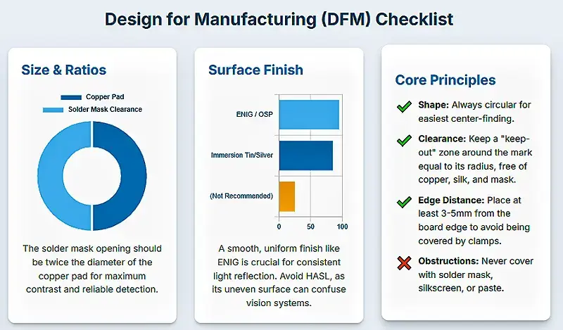
The optimal fiducial shape is a solid filled circle. A circular shape maintains a consistent geometric center regardless of the angle of rotation, greatly simplifying the machine vision algorithm's fast and accurate centroid recognition. Furthermore, in low-complexity or prototyping scenarios, circular mounting holes can be utilized as temporary or auxiliary fiducial points, provided they meet clearance and visibility requirements, although their stability and accuracy are generally inferior to standard bare copper pads.
IPC/SMEMA guidelines for size are clear:
Common Engineering Practice: 1.0 mm bare copper + 3.0 mm solder mask opening; or 1.6 mm bare copper + 3.2 mm opening.
The physical characteristics of a fiducial mark directly determine the performance of the machine vision system. They must be areas of bare copper to maximize optical contrast and minimize surface unevenness.
Physical Requirements:
The stringent flatness requirement (below 15 microns) is key to achieving high-precision assembly. Modern SMT equipment, particularly 3D Solder Paste Inspection (3D SPI) systems, rely on precise Z-axis positioning (height) for measurement. The fiducial points act as the Z-axis zero reference plane in this process. If the fiducial itself is uneven, the reference plane established by the machine during optical measurement will be unstable. Therefore, fiducial quality directly dictates the accuracy and reliability of SPI paste height measurements, a non-negotiable requirement for the most stringent IPC Class 3 applications.
The Clearance Area, also known as the Keepout Zone, is designed to ensure that the specific area surrounding the fiducial mark is completely free of other circuit features, silkscreen, text, or markings, preventing interference with the vision system's recognition.
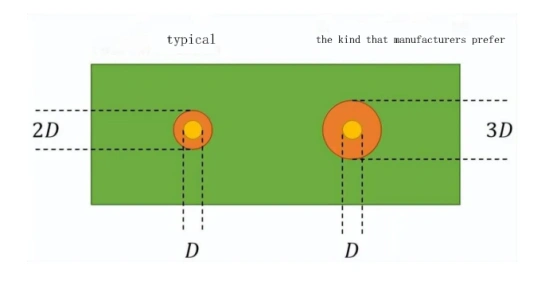
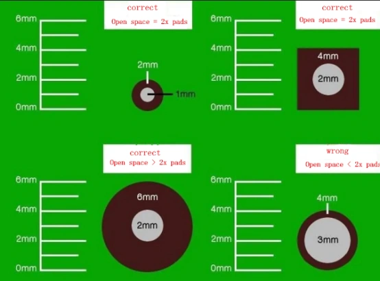
Clearance Specifications:
In practice, designers typically achieve this specification by creating a 1.0 mm solid copper pad in the PCB design software and opening a 3.0 mm window in the solder mask layer. Furthermore, plane pours are acceptable underneath the fiducial mark on inner layers, as this "floating" pad has no electrical net connection and will not adversely influence the performance of the copper pour below.
Table 1: IPC/SMEMA Fiducial Mark Core Design Specifications
| Specification Element | Design Requirement | Standard Basis | Importance |
|---|---|---|---|
| Shape | Solid Filled Circle | IPC/SMEMA | Rotational invariance, easy centroid recognition |
| Minimum Diameter | 1.0 mm (0.040 in) | IPC/SMEMA | Ensures sufficient contrast area |
| Maximum Diameter | 3.0 mm (0.120 in) | IPC/SMEMA | Avoids excessive PCB area usage |
| Size Consistency | Variation on the same board ≤ 25 μm (0.001 in) | IPC | Uniformity of machine vision parameters |
| Surface Flatness | ≤ 15 μm (0.0006 in) | IPC/SMEMA | Z-axis measurement baseline accuracy |
| Clearance Diameter (DC) | Preferred 3 × DF | Machine Vision Performance Optimization | Ensures high-contrast area without interference |
To meet the requirements of different assembly stages and precision levels, fiducial marks are classified into distinct levels:
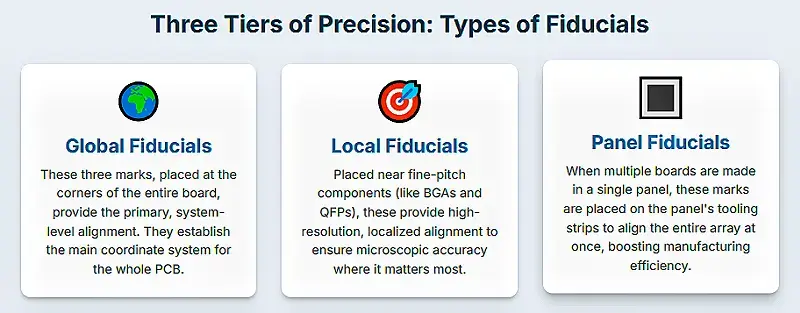
1. Panel Fiducials: These marks are placed on the tooling strips/frames of the SMT panel and are used to align the entire panel with the stencil printer and placement machine at the beginning of the production line. > Panel Requirement for Assembly
2. Global Fiducials: Located in the diagonal corners of the individual PCB, they are used to precisely locate the entire board relative to the assembly equipment's position and orientation.
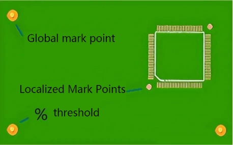
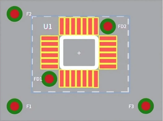
3. Local Fiducials: Located near individual fine-pitch components (typically pitch less than 20 mils), usually on the outer corners of the component land pattern. They are specifically used to compensate for minute localized deviations caused by manufacturing tolerances or thermal stress, providing the highest positional accuracy for that component. Note that local fiducials cannot be used for stencil print alignment; they only function during the component placement phase.
> Recommend reading: Fundamentals of PCB Thermal Design | NextPCB
The number of fiducial marks is a critical decision point for achieving different levels of geometric correction capability.
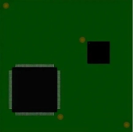
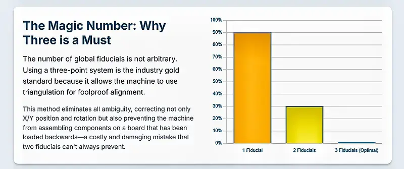
Table 2: Comparison of Fiducial Quantity and Geometric Correction Capability
| Fiducial Quantity | Correction Capability | Applicable Scenario | Depth of Geometric Compensation |
|---|---|---|---|
| 2 (Minimum Global) | X/Y Translation, θ Rotation | Low precision, small boards | Cannot correct non-linear distortion |
| 3 (Optimal Global/Panel) | X/Y Translation, θ Rotation, Non-linear (Stretch/Twist) Compensation | All standard SMT, high precision, large PCBs, double-sided assembly | Capable of compensating for Z-axis planar distortion |
| Local (Component-Level) | Local X/Y/θ fine-tuning | Fine-pitch components (< 20 mils) | Highest accuracy, used only for placement |
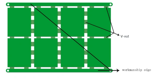
Fiducial marks must be placed outside a safe distance from the PCB edges to ensure they are not obscured or damaged by the clamping fixtures or conveyor rails used in the automated assembly line.
The SMEMA standard requires that the distance from the fiducial center to the PCB edge must be no less than the sum of the SMEMA standard transport clearance (7.62 mm / 0.300 in) and the minimum required fiducial clearance.
In practical design, the following typical values are often followed:
Fiducial marks must be located completely within the board, away from any structure that might be covered by clamps, ensuring they can be clearly recognized by the machine vision system during any assembly stage.
In panel design, V-Cut (V-Score) lines or Tab-Route (stamp hole) structures are used for the final separation of individual boards. These separation operations generate momentary mechanical stress that can lead to cracking of nearby solder joints or compromise the reliability of precision components.
Fiducial marks must be kept away from these stress zones. Industry guidelines recommend placing components at least 5 mm (0.2 inches) away from the scored edge. For fiducial marks, a similar, or even stricter, safety distance should be adopted. For instance, on thinner PCBs (e.g., 0.6–0.8 mm), which are more prone to bending and cracking, a larger keepout zone of 5–7 mm is advisable. Ensuring the fiducial points are located away from the separation stress sources is crucial for maintaining their positional accuracy.
The recognition performance of machine vision systems is directly related to the efficiency of their image processing algorithms, and high contrast is the decisive factor in ensuring image quality and fast recognition.
The design of the fiducial mark must provide a stable, high-contrast environment:
Through this design, the machine vision system can rely on consistent light reflectivity characteristics to quickly and accurately locate the fiducial mark's centroid.
The choice of PCB Surface Finish affects the fiducial mark's flatness, brightness, and light reflectivity, which in turn influences the machine vision system's alignment accuracy.
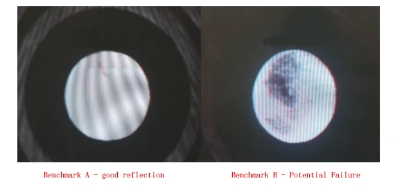
It is important to note that different surface finishes (e.g., Tin-Lead on HASL or Nickel-Gold on ENIG) have different light reflectivity characteristics. Advanced SMT placement machines and 3D SPI systems must adjust their illumination configurations (e.g., top lighting, slanted lighting) based on the board type and surface finish. This optimization is necessary to acquire high-quality 2D grayscale images for accurately identifying fiducial marks and distinguishing between pads and solder paste during inspection.
Fiducial marks play an indispensable role in the 3D SPI process. SPI checks the area coverage, height, and volume of the solder paste, making it one of the most vital quality control steps on the SMT production line.
Modern SPI technology relies on combining 2D grayscale images and 3D height maps:
The machine must first align using the fiducial points before it can accurately measure the height of the solder paste relative to the pad surface. Only by capturing the true height and grayscale information of each point can SPI accurately differentiate actual solder paste from other board features (like silkscreen or thin paste smears), thereby identifying critical defects such as insufficient paste or shorts. The high flatness requirement for fiducial marks is the fundamental guarantee for the SPI system to establish a precise Z-axis baseline.
Flexible circuits (Flex Circuits) and rigid-flex boards follow the IPC-2223 standard. Flexible materials (such as polyimide) exhibit unique physical characteristics during manufacturing processes like cutting, etching, baking, and thermal cycling, specifically significant stretch, shrinkage, and non-uniform deformation (anisotropy). This "floating" of the material can cause unpredictable deviation of the fiducial marks relative to their designed coordinates, directly compromising component placement accuracy.
To overcome this inherent instability of flexible materials, the fiducial mark design must include additional reinforcement measures. Designers must ensure the fiducial mark does not float independently on the polyimide layer but is anchored to a substantial copper area:
Since the anisotropic shrinkage of flexible materials is an unavoidable physical property, advanced flexible circuit manufacturers must introduce dynamic compensation mechanisms during the process flow.
The principle is as follows: early in the manufacturing process, equipment measures the fiducial marks located on the outer corners of the panel to determine the actual amount of stretch or shrinkage that occurred in the X and Y axes, known as the Scaling Factors. These scaling factors, calculated via optical measurement, are then used for software compensation to dynamically adjust subsequent manufacturing steps (such as drilling program coordinates or stencil dimensions). This fiducial-based software compensation is an advanced manufacturing practice essential for ensuring high-precision assembly of flexible PCBs.
The IPC-A-610 standard determines the acceptability of electronic assemblies, with Class 3 representing the highest level of quality and reliability. This class applies to critical applications—such as aerospace, medical, and automotive electronics—where failure is zero-tolerance.
While IPC-A-610 primarily focuses on final acceptance criteria like solder joint quality and component placement, achieving the ultra-high positional accuracy required by Class 3 necessitates stringent control at the manufacturing foundation. This means fiducial marks must strictly comply with micrometer-level tolerance requirements, including the 15 μm surface flatness limit and the 25 μm size consistency limit. Only when these optical reference points possess absolute quality and precision can the subsequent placement and SPI processes meet the zero-defect standard required by IPC Class 3.
Design flaws are a frequent cause of yield reduction in automated assembly. Experienced engineers must be vigilant in the design phase to avoid the following common errors:
> Recommend reading: Practical DFM Checklist and HQDFM Practice
PCB fiducial marks are the key physical elements for successful automated SMT assembly; they are far more than simple dots on a design file. Top-tier design practice requires designers to deeply understand the dual role of the fiducial mark as both the mathematical foundation and the physical reference point for the machine vision system.
A successful fiducial strategy must integrate materials science, geometry, and advanced manufacturing processes:

While fiducial marks are currently the standard and mandatory method for ensuring the highest SMT placement accuracy, the industry is exploring the possibility of relying purely on component features for alignment (Feature-based Alignment). However, existing research suggests that post-hoc feature-based alignment methods have limitations in reliability when dealing with unforeseen distribution shifts and qualitatively different displacements of components at various spatial locations.
Therefore, for the foreseeable future, especially in safety-critical applications requiring extreme reliability (such as aerospace, medical), fiducial marks will remain the critical and mandatory technology for guaranteeing the highest placement precision and process reliability. The combination of fiducial marks with advanced computer vision algorithms (for processing 2D/3D images) provides the most robust and reliable positioning foundation, ensuring the automated assembly line can consistently produce electronic assemblies that meet the IPC Class 3 standard.
If you are designing the next generation of high-precision PCBs and want to ensure your fiducial marks fully comply with IPC Class 3 and the highest automation assembly requirements, NextPCB offers professional manufacturing and assembly (PCBA) services. Submit your design files now to get a quote and equip your product with top-tier manufacturing reliability right from the design stage.

Still, need help? Contact Us: support@nextpcb.com
Need a PCB or PCBA quote? Quote now

