NextPCB Capabilities
Printed Circuit Boards
NextPCB Capabilities
Printed Circuit Boards
 PCB Assembly
 Layer Buildup
 SMD-Stencils
 PCB Design-Aid & Layout
 Mechanics
 Quality
 Drills & Throughplating
 Factory & Certificate
 PCB Assembly Factory Show
Certificate
PCB Assembly Factory Show
Certificate
Support Team
Feedback:
support@nextpcb.com


In this article, we're going to explore "What is an Open Circuit?" We'll examine open circuit resistance, compare open circuit vs short circuit, and check out real-life examples — including how open circuits appear in PCB manufacturing and SMT assembly. An open circuit refers to a break or interruption in an electrical circuit that prevents current from flowing. Whether you are a student encountering the concept for the first time, an EE debugging a PCB trace fault, or a manufacturing engineer analyzing an SMT assembly defect, this guide gives you the physics, the practical diagnosis workflow, and the design practices you need.
Quick physics framing: In the ideal open-circuit state, current is strictly zero (I = 0), yet a non-zero terminal voltage can exist — called the open-circuit voltage VOC. Because P = V × I, steady-state power dissipation at the break is zero. These fundamentals underpin both safe diagnosis and circuit analysis methods such as forming a Thévenin equivalent.
An open circuit is an electrical circuit in which the current path is broken, so current cannot flow. For current to move through a circuit, it requires a continuous, closed loop from the supply's positive terminal, through the load, and back to the negative terminal. Any interruption in that loop — a lifted pad, an open switch, a severed wire — creates an open circuit.
Two key quantities define the open-circuit state:
This separation of V and I is what makes an open circuit conceptually distinct from a de-energized circuit. A de-energized circuit has both V = 0 and I = 0 (the supply itself is off). An open circuit under a live supply has VOC ≠ 0 and I = 0 simultaneously — a distinction that matters when diagnosing faults safely.
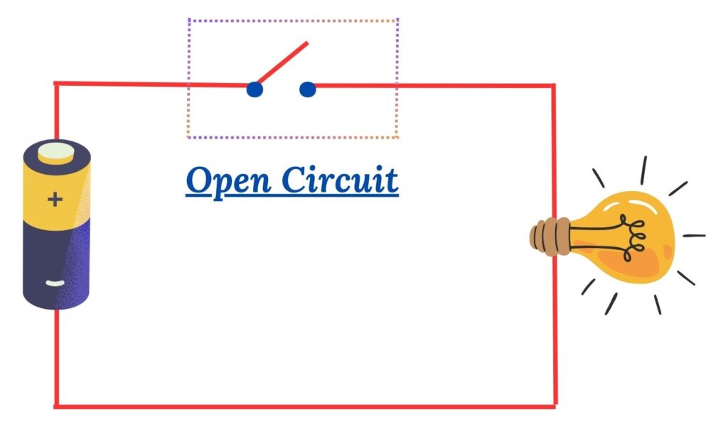
Open Circuit Diagram — the gap prevents current flow while voltage remains present across the break.
Components Free Worldwide Shipping
Ohm's Law relates voltage (V), current (I), and resistance (R):
V = I × R → R = V / I
In an open circuit, I = 0. Substituting:
R = V / 0 → ∞
Infinite resistance is the ideal model: the gap between the two open terminals presents no conductive path whatsoever. In practice, two separated conductors form a small parasitic capacitance Cp and an extremely large (but finite) leakage resistance RL in parallel. At DC and low frequencies the isolation is effectively complete. As frequency increases, the capacitive reactance XC = 1 / (2πf Cp) decreases, allowing a small AC displacement current to pass. This is normally negligible in power and signal work, but becomes relevant in RF PCB design and high-speed digital traces, where even a mechanically open pad can couple noise.
A digital multimeter placed across a genuinely open circuit will display "OL" (overload/out of range) in resistance mode, confirming that resistance exceeds its measurement range — consistent with the theoretical infinite value.
For a deeper look at Ohm's Law and related divider circuits, see: Voltage Dividers: Operations and Functions.
Open circuits arise from three broad categories of root cause: component and conductor failure, external environmental factors, and human error. Understanding which category applies shapes both the remediation strategy and any preventive action.
Physical deterioration of conductors or components is the most common source of unintentional open circuits.
For electronics manufacturing engineers, open circuits are one of the highest-frequency defect categories encountered during PCB fabrication, SMT assembly, and in-circuit test (ICT). Unlike a short circuit — which usually trips a fuse or trips ICT immediately — an open circuit can be latent: the board may pass functional test at room temperature under light load, then fail in the field under vibration or thermal stress. Understanding the root causes specific to each manufacturing stage is essential for both yield improvement and IPC-A-610 conformance.
Surface-mount technology assembly introduces several additional open-circuit failure modes that are distinct from fabrication issues:
The IPC and IATF 16949 supply chain require layered electrical test coverage to catch opens at each stage:
| Test Stage | Method | Open Circuit Coverage |
|---|---|---|
| Bare board | Bare-board electrical test (BBET) — flying probe or fixture | Trace continuity, via continuity, no access to component pads |
| Post-paste | Solder paste inspection (SPI) | Detects insufficient paste → predicts missing joints before reflow |
| Post-reflow | Automated optical inspection (AOI) | Detects lifted components, gross tombstoning, visible missing solder |
| BGA / QFN | X-ray inspection (AXI) | Detects voided or missing balls hidden under package |
| Final assembly | In-circuit test (ICT) / flying probe | Electrical opens across all nets; identifies exact net location |
| Functional | Functional test (FCT) | Confirms system-level behavior; may miss latent opens at low test stress |
Get Instant PCB Quote Engineer Consultation
A PCB trace crack is one of the most insidious forms of open circuit because it is often invisible under normal optical inspection. The crack may be only a few microns wide — the copper is physically severed, current cannot flow, but the fracture is too narrow for the eye (or even a 10× loupe) to resolve. Trace cracks are a leading cause of intermittent field failures and are disproportionately common in boards that experience mechanical flexure, thermal cycling, or both.
Standard detection methods for trace cracks include:
In discrete and integrated electronics, the open-circuit condition is not always a failure — it is often the intended operating state of a semiconductor device. Two examples are particularly instructive.
A bipolar junction transistor (BJT) has three operating regions: active, saturation, and cut-off. In cut-off, the base-emitter voltage VBE is below the forward-bias threshold (roughly 0.6 V for silicon). Both junctions are reverse-biased, the depletion regions are wide, and essentially no minority carriers are injected into the base. The result:
The transistor in cut-off behaves as an open circuit between collector and emitter. This is the "off" state in digital logic and switching power supplies. The transistor switch is open; the load is disconnected from the supply.
When a diode is reverse-biased — that is, the cathode is at a higher potential than the anode — the internal depletion region widens. The potential barrier prevents majority carriers from crossing, and only a very small reverse saturation current IS (typically nanoamperes for silicon) flows. For most practical circuit analysis, a reverse-biased diode is treated as an open circuit.
This behavior is exploited deliberately in many applications: rectifier circuits rely on diodes being open to reverse half-cycles; clamping and protection circuits use reverse-biased diodes to block until a threshold is exceeded; and PIN diodes controlled by a bias voltage switch entire RF signal paths open or closed.
Understanding that open circuits can be either unintentional faults or designed-in switching states is essential for reading schematics and interpreting circuit behavior correctly.
Open circuits and short circuits are the two fundamental fault types in electrical engineering, and they produce opposite electrical signatures. A closed (normal operating) circuit sits between them.
In an open circuit, the current path is broken and I = 0. The full source voltage appears across the break as VOC, but no power is dissipated at the fault location. A short circuit is the opposite: an unintended low-resistance path forms between two nodes, forcing I to a very high value while the terminal voltage collapses toward zero. The power P = I²R concentrated in the short can be destructive within milliseconds.
Open Circuit vs. Short Circuit vs. Closed (Normal) Circuit
| Parameter | Open Circuit | Short Circuit | Closed (Normal) |
|---|---|---|---|
| Resistance | → ∞ | → 0 | Finite RL |
| Current | I = 0 | Very high (limited by source impedance) | I = V / RL |
| Terminal Voltage | ≈ VOC | ≈ 0 | Distributed per network |
| Power at fault | 0 | Very high I²R — potentially destructive | Useful I²RL |
| DMM resistance reading | OL (overload) | 0 Ω or near-zero | Expected RL |
| DMM voltage reading (live) | ≈ Supply voltage across break | ≈ 0 V across fault | Distributed per design |
| Immediate hazard | Loss of function; context-dependent voltage hazard | Overheating, fire risk, component damage | Normal operation |
| Fuse response | No overcurrent — fuse intact | Overcurrent — fuse blows (if rated correctly) | Normal current — fuse intact |
| PCB-level root cause examples | Cracked trace, missing solder, lifted pad, blown fuse | Solder bridge, conductive contamination, insulation breakdown | — |
Safety note: While opens generally produce no local heating (P = 0), they are not uniformly safe. Two contexts make open circuits hazardous: (a) an open neutral in a split-phase residential system can place excessive voltage across loads on the remaining hot conductor; (b) opening an inductive load (motor, relay coil, transformer) while current is still flowing generates a high-voltage transient from V = −L dI/dt. Both scenarios require circuit protection measures beyond simply treating the open as "inactive."
Locating an open circuit efficiently requires matching the diagnostic tool to the nature of the fault and the system architecture. Work systematically from coarse to fine rather than probing randomly.
Before reaching for instruments, a careful visual scan finds a significant proportion of opens: lifted pads, cracked solder joints, burnt components, connector pins that have receded into their housing, or wires that have pulled free of terminals. Use adequate lighting and a 10× loupe or digital microscope for PCB inspection. On through-hole assemblies, inspect the solder-side joints; on SMT assemblies, look for lifted component edges, especially on large chip capacitors and BGAs.
With the circuit de-energized, a DMM in continuity mode will emit an audible tone for a resistance below approximately 30 Ω and display "OL" across an open. This is the fastest method for tracing single-conductor faults:
For opens in energized systems, a DMM in voltage mode is safer than probing with continuity. The full source voltage appearing across a junction, connector, or switch that should be conducting indicates an open at that point. A voltage drop of zero across a component expected to have a drop (e.g., a fuse) confirms the component is passing current normally; the full supply appearing across it confirms it is open.
An oscilloscope is useful when the open is intermittent or signal-integrity related. By observing waveform shape and amplitude at successive points along a signal chain, you can identify where a signal disappears — narrowing the fault location to a single stage or even a single component. A signal that appears normal on one pin of a connector but is absent on the mating connector pin confirms an open contact.
For long cables, high-speed PCB traces, or backplane interconnects where physical access is limited, TDR sends a fast electrical pulse down the conductor and measures the reflected echo. An open termination reflects the pulse with the same polarity; the time delay between the transmitted and reflected pulses gives the distance to the fault with meter-level precision. TDR is the standard diagnostic method for cable harness opens in automotive, aerospace, and telecommunications applications.
When the open is a high-resistance connection rather than a complete break — a corroded contact, a partially fractured trace — the elevated resistance causes localized heating under load. An infrared camera or non-contact thermometer can identify hot spots that would be invisible to a continuity test run at low test current.
A digital multimeter (DMM) is the most accessible tool for open circuit diagnosis. The following step-by-step workflow covers both de-energized continuity testing and live-circuit voltage probing — the two modes most relevant to electronics troubleshooting.
When to use: PCB trace faults, solder joint opens, cable harness opens, fuse testing.
When to use: Tracing opens in live power circuits, switch and connector faults, fuse verification under load.
| Scenario | DMM Mode | Open Circuit Reading | Good Circuit Reading |
|---|---|---|---|
| Wire / PCB trace | Continuity (Ω) | OL / no beep | Beep / <1 Ω |
| Fuse | Continuity (Ω) | OL / no beep | Beep / <1 Ω |
| Switch (open/off) | Continuity (Ω) | OL (expected) | Beep when closed |
| Fuse (under power) | Voltage (V) | ≈ supply voltage across fuse | ≈ 0 V across fuse |
| Connector pin pair (live) | Voltage (V) | Voltage on one side, 0 V on other | Same voltage both sides |
| PCB net (de-energized) | Resistance (Ω) | OL between net endpoints | <10 Ω end-to-end |
Engineer Consultation Get Instant PCB Quote
Not every open circuit represents a failure. Many circuit functions depend on deliberately created open conditions.
A switch in the "off" position is, by definition, an open circuit. The mechanical contacts are separated; I = 0; the load is disconnected. This is the simplest and most universal application of a controlled open circuit. Relays extend this to remote or electrically isolated switching: the coil energizes to close (or open, in normally-closed configurations) a separate contact set.
Both devices are designed to create an open circuit under fault conditions. A fuse contains a calibrated conductor that melts when current exceeds its rating, permanently opening the circuit. A circuit breaker does the same but with a resettable mechanical mechanism. In both cases, the open circuit is the protective outcome — it stops destructive current flow before damage propagates to more expensive components.
Many sensors operate by switching a circuit between open and closed states based on a physical condition:
As discussed in the transistor section, a BJT in cut-off or a MOSFET with VGS below its threshold voltage presents a high-impedance (effectively open) path between drain and source. Digital logic is built on this controlled switching between near-open and near-short states. The "high-Z" or tri-state output of a logic device is an intentionally open output, used when multiple drivers share a bus and only one may be active at a time.
Battery state-of-charge measurement frequently relies on VOC: with the load disconnected (open circuit), the terminal voltage reflects the electrochemical potential of the cell more accurately than under load. Solar cell characterization similarly uses VOC as one of the two primary performance metrics (along with short-circuit current ISC).
Unintentional open circuits are largely preventable through sound design, manufacturing, and maintenance practices. The following measures apply at different stages of a product's lifecycle.
When designing circuits that switch inductive loads (relays, solenoids, motors), always provide a freewheeling path for the stored energy when the switch opens. For DC circuits, a flyback diode placed across the load in reverse orientation provides a low-impedance path for the collapsing magnetic field, clipping the voltage transient. For higher energy or faster transients, a TVS diode or MOV with a voltage rating slightly above the supply can absorb the spike. Omitting this protection is one of the more common causes of switch contact or MOSFET gate destruction.
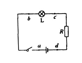
A battery, a switch, and a lamp connected in series is the standard introductory open-circuit example, but it is worth examining carefully because each state teaches something distinct.
Switch open (off): The circuit is open at the switch contacts. I = 0; the lamp does not light. A voltmeter across the switch reads the battery voltage (VOC), confirming the source is present. A voltmeter across the lamp reads approximately zero — because no current flows, there is no voltage drop across the lamp's resistance.
Switch closed (on): The path is complete. Current flows according to I = Vbattery / (Rswitch + Rlamp). The lamp illuminates. The switch, ideally a zero-resistance contact, drops negligible voltage; nearly all of Vbattery appears across the lamp.
Wire break (fault open): If the wire between the battery and lamp is severed, the lamp also goes dark and I = 0. However, now the full battery voltage appears across the break, not across the switch. A continuity check from one wire end to the other shows "OL," locating the fault.
Inductive extension: Replace the lamp with a relay coil. When the switch opens while current is flowing through the coil, V = −L dI/dt can produce a spike of tens to hundreds of volts across the switch contacts, causing arcing and contact erosion. A flyback diode across the relay coil suppresses this by providing an alternative current path.
A closed circuit has a complete, uninterrupted path from the supply through the load and back. Current flows and the load operates normally. An open circuit has a break in that path; current is zero and the load is inactive. The term "open" refers to the gap in the path, analogous to an open door that blocks passage.
In resistance or continuity mode: "OL" (out of limit / overload), indicating resistance exceeds the instrument's range — consistent with theoretical infinite resistance. In voltage mode, with the circuit energized: approximately the source voltage, because the full supply potential appears across the break.
Generally, an open circuit stops current flow and removes power from the load, which is often the safe outcome. Two situations make opens hazardous: (1) opening an inductive load under current creates a voltage transient that can damage semiconductors or arc across switch contacts; (2) an open neutral in AC power distribution can cause abnormal voltages across connected loads. In both cases, the hazard comes from system context, not from the open itself.
A BJT in cut-off mode (VBE below threshold) or a MOSFET with VGS below its threshold voltage presents a very high impedance between its current-carrying terminals. For circuit analysis, this is treated as an open circuit. Digital logic exploits this: the transistor is "off" (open) for a logic 0 output and "on" (near-short) for a logic 1 output.
VOC is the terminal voltage of a source when no current is drawn — that is, when the external circuit is open. It represents the maximum potential a source can deliver. For a battery, VOC is used to estimate state of charge. For a solar cell, VOC is one of the two main performance parameters on an I-V curve.
Intermittent opens are typically caused by: loose connector contacts that make and break with vibration; cracked solder joints that open under thermal expansion and close when cool; or fractured PCB traces that open when the board flexes. They are among the most difficult faults to diagnose because they may not be present during bench testing — TDR, flexing the board while monitoring continuity, or thermal cycling while measuring resistance are commonly used to expose them.
Open circuits are used deliberately in Thévenin's theorem: to find the Thévenin equivalent voltage VTh, you calculate or measure the open-circuit voltage at the terminals of interest with the load removed. This simplifies complex networks to a single voltage source and series resistance for analysis of load behavior.
In PCB and SMT manufacturing context: an open circuit is a missing or broken connection — caused by cracked traces, lifted pads, missing solder, or BGA voids — meaning current cannot flow where it should. A short circuit is an unintended connection between two nets — caused by solder bridges, conductive contamination, or trace spacing violations — meaning current flows where it should not. Both are detected by bare-board electrical test (BBET) and in-circuit test (ICT), but their root causes and corrective actions differ substantially.
Start with visual inspection under magnification for lifted pads or visible solder cracks, then use a DMM in continuity mode to check net endpoints. For BGAs or hidden opens, use X-ray inspection. For intermittent opens, thermal cycling while monitoring resistance or a four-wire Kelvin measurement at milliohm resolution can expose cracks invisible to standard continuity testing. TDR is effective for locating opens in long cable harnesses or high-speed PCB traces.
An open circuit is defined by the absence of a complete current path: I = 0, while VOC may be non-zero. At the fault location, power dissipation is zero — the open is non-destructive in itself — but the system consequences depend heavily on context: loads stop functioning, inductive switching can produce hazardous transients, and abnormal voltage distribution in certain power configurations can create over-voltage conditions.
Open circuits arise from physical failure (broken wires, cracked solder joints, corrosion, blown fuses), external disruptions (power outages, ESD), or human error (incorrect wiring, missed solder). In PCB manufacturing and SMT assembly specifically, opens trace to fabrication defects (under-etching, drill breakout, via plating voids), paste and reflow process failures (tombstoning, cold joints, insufficient paste coverage), and hidden joint defects in BGA/QFN packages that require X-ray to detect. They also appear by design in switches, fuses, transistors in cut-off, and reverse-biased diodes — contexts where "open" is the intended operating state, not a fault.
Effective detection works through a layered approach: visual inspection first, followed by DMM continuity checks, voltage measurement under power, oscilloscope signal tracing, TDR for long conductors, and thermal imaging for high-resistance connections. Prevention at the design stage — adequate trace width, teardrop vias, DFM review, proper inductive load protection, and accessible test points — is substantially more cost-effective than field diagnosis and repair.
Key design checkpoints:
Engineer Consultation Get Instant Online PCB Quote

Still, need help? Contact Us: support@nextpcb.com
Need a PCB or PCBA quote? Quote now


 Surface