

 NextPCB Capabilities
 PCB Assembly
 Layer Buildup
 SMD-Stencils
 PCB Design-Aid & Layout
 Mechanics
 Surface
 Quality
 Drills & Throughplating
 Factory & Certificate


In modern electronics manufacturing, the Surface Mount Technology (SMT) assembly process plays a pivotal role in ensuring the efficiency, durability, and quality of electronic products. This guide provides a comprehensive overview of the printed circuit boards assembly (PCBA) manufacturing workflow, incorporating real factory practices, industry standards, and critical quality control points at each stage.
As a professional PCB and PCBA manufacturer with over 10 years of experience, NextPCB has witnessed firsthand how a robust and meticulously tested assembly process can determine the success or failure of an electronic product launch.
In this blog, we'll walk you through the end-to-end PCBA process—from sourcing electronic components to final functional test—to help you understand how to achieve reliable assembly outcomes.
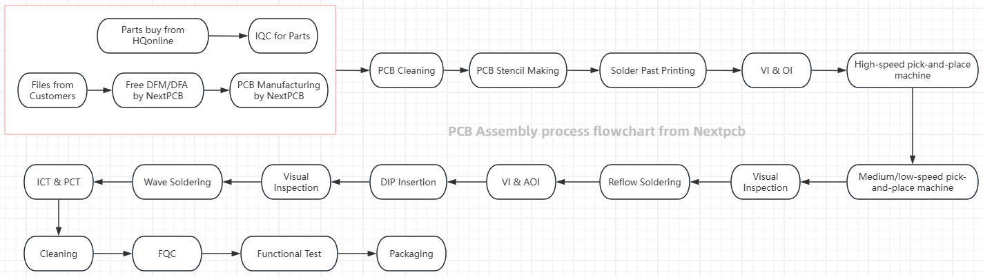
PCB assembly process flowchart
Step 1. Component Procurement with HQOnline
The first step in the PCBA production process involves sourcing all necessary electronic components that align with the design specifications and Bill of Materials (BOM). Selecting reliable suppliers and confirming delivery schedules are essential to prevent production delays and ensure component authenticity.
To streamline this process, HQOnline offers a comprehensive solution. As a subsidiary of Shenzhen Huaqiu Electronics Co., Ltd., the same parent company as NextPCB, HQOnline provides access to over 600,000 components from more than 3,000 international and Asian brands. Their platform ensures 100% authenticity by sourcing parts directly from original manufacturers or authorized distributors, eliminating concerns about counterfeit or refurbished components.
Additionally, NextPCB's free BOM service allows you to batch search up to 200 electronic components, providing real-time pricing and availability, and enabling efficient BOM management. With same-day dispatch to over 160 countries and free international shipping on orders over $50, we offers a seamless and cost-effective procurement experience.
By leveraging our extensive inventory and user-friendly platform, you can ensure timely and reliable sourcing of components, setting a solid foundation for the subsequent stages of the PCBA production process.
Make Eyerything Under Control: Turnkey PCB Assembly Services at NextPCB
> Recommend reading: Common Components on a PCBA and What Matters in Assembly
Step 2. Incoming Quality Control (IQC)
After receiving the components, a thorough Incoming Quality Control (IQC) is carried out. This includes verifying part numbers, quantities, and component conditions to rule out any defects. Moreover, implementing Electrostatic Discharge (ESD) protocols is vital to protect sensitive integrated circuits and other components during handling.
Step 3. PCB Cleaning
Before solder paste application, it's crucial to clean the PCB using appropriate cleaning agents. This step removes oils, dust, and residues that may affect the adhesion of solder paste and the reliability of solder joints during reflow soldering.
Step 4. PCB Stencil Making
A precision-designed stencil ensures uniform and accurate application of solder paste. Stencil apertures must align exactly with SMT pads, and any defect in stencil fabrication can compromise the entire SMT assembly.
Step 5. Solder Paste Printing
Solder paste application is a cornerstone of surface mount technology (SMT). The quality of solder paste printing directly impacts soldering effectiveness. The paste should be applied uniformly with the right squeegee pressure, and its management is critical to maintaining quality:
- The paste must be refrigerated between 0-10°C when not in use.
- The container should always be sealed tightly.
- Avoid leaving paste on the stencil for over 30 minutes to prevent degradation.
- Before use, it must be brought to room temperature for at least 2 hours and stirred for 3-5 minutes in the same direction using a tool with rounded edges to avoid damaging the solder balls.
- The paste must be consumed within 24 hours of opening to maintain its effectiveness.
> Recommend reading: Circuit Board Solder: Types, Temperatures & How to Choose (Reflow & Hand Soldering Tips)
Step 6. Visual Inspection/Optical Inspection
After printing, conduct visual inspection and optical inspection (AOI) to verify the evenness and alignment of solder paste on all SMT pads. This stage sets the stage for flawless pick and place machine operations.
Step 7. High-Speed Pick-and-Place Machine Operation
High-speed pick-and-place machines are used to accurately mount small electronic components. It is vital to ensure that the machine settings are correct and that the orientation and position of the components are accurate to avoid misplacement. Key points include:
- High-speed machines typically feature 10 to 15 placement heads, with each head capable of swapping 2 to 5 nozzles for different components.
- The components are picked up using vacuum suction technology.
- Component placement rate up to 10 per second.
- Depending on the cycle time of the bottleneck workstation, 1 to 3 machines are usually installed per SMT production line.
- Prepare 10 extra parts per type to compensate for potential misfeeds.
- High-speed machines can experience material wastage (component misfeeds), particularly with loose or scattered parts. Therefore, during the sample production phase, it's recommended to prepare extra components. A buffer of around 10 additional pieces beyond the actual production count is advisable to account for such wastage.
This step is critical for ensuring precise placement of integrated circuits and passive components in SMT assembly.
Step 8. Medium to Low-Speed Pick-and-Place Machine Operation
Following high-speed placement, mid-to-low-speed machines handle larger or special-shaped components.
For general-purpose pick-and-place machines, they typically feature 3 to 5 placement heads, each capable of swapping 2 to 5 nozzles. These machines can place 1 to 2 components per second from tape reels and take 1 to 3 seconds for components from trays. This ensures complete component mounting before soldering. Generally, each SMT production line is equipped with one of these machines.
Step 9. Pre-Reflow Inspection
A pre-reflow visual inspection is conducted to identify misaligned, missing, loss, or improperly seated parts before the board enters the reflow oven.
Step 10. Reflow Soldering
Reflow soldering is the core of SMT technology. It requires the appropriate temperature profile to be set. It is important to avoid overheating or poor cooling of solder joints to prevent defects.
The temperature profile is segmented into four key zones within the reflow oven: the preheat zone, thermal soak zone, reflow zone, and cooling zone. Each zone has specific temperature control requirements to ensure the quality of the solder joints and the reliability of electronic components.
1. Preheat Zone: Gradual heating to evaporate solvents and activate flux.
When the PCB enters the preheat zone, the solvents and gases in the solder paste evaporate. At the same time, the flux in the solder paste begins to wet the pads, component terminals, and leads. The solder paste softens, collapses, and covers the pads, isolating them from oxygen.
2. Soak Zone: Uniform heating to prevent thermal shock to electronic components.
As the PCB enters the thermal soak zone, it is preheated thoroughly to prevent damage to the PCB and components from a sudden rise in temperature when entering the reflow zone.
3. Reflow Zone: Melting of solder paste to form solid solder joints.
When the PCB reaches the reflow zone, the temperature rises rapidly, causing the solder paste to melt. The liquid solder wets, diffuses, and flows over the pads, component terminals, and leads, forming a solid solder joint.
4. Cooling Zone: Controlled cooling to solidify solder and prevent cracks.
Finally, the PCB enters the cooling zone, where the solder joints solidify, completing the reflow soldering process.
Maintaining an optimal profile is essential for reliable solder joints and overall PCB integrity.
Step 11. Visual Inspection and Automated Optical Inspection (AOI)
Post-reflow, both manual inspection and automated optical inspection (AOI) systems are used to ensure solder joint quality and detect issues such as:
Cold Solder Joint
The solder joint appears visually acceptable but does not actually contact the component leads or pads. This defect may occur due to insufficient melting of the solder or inadequate wetting of the soldering area. Components with cold solder joints may fail to establish electrical connections, resulting in functional failure.
Solder Bridging
Excess solder appears between component leads, causing a short circuit.
Dry Joint/Cold Solder
The solder joint is not secure and may result from insufficient temperature or inadequate soldering time, leading to poor electrical contact.
Component Misalignment
Components may shift during the soldering process, resulting in incorrect positioning.
Solder Balls
Small solder balls may form during the soldering process, posing a risk of short circuits.
Missing/Incorrect Components
Certain components may not be correctly placed or may be replaced with incorrect components.
Poor Solder Joint
The solder joint may be excessively large or small, or its shape may be irregular, potentially affecting electrical performance.
Irregular solder shapes
This occurs when the solder joint deviates from the intended form, potentially affecting electrical conductivity and mechanical strength, and can be caused by inconsistent solder paste application or improper soldering techniques.
Step 12. DIP Insertion (Through-Hole Components)
Through-hole component (hole component) insertion requires precise alignment and depth control. Considerations during the DIP insertion process inlcude:
Maintain Cleanliness
Before insertion, check the surfaces of electronic components for contaminants such as grease or paint. Ensuring that the surfaces are clean is crucial to avoid compromising the quality of insertion and soldering.
Flat Placement and Orientation
During the insertion process, ensure that the electronic components are flat against the PCB. After insertion, verify that the components are level and not uneven. Additionally, components with directional indicators must be inserted according to their specified orientation to prevent incorrect placement.
Avoid Obstructing Pads
Ensure that the inserted leads do not obstruct the pads to guarantee the quality and reliability of soldering.
Control Insertion Force
Be mindful of the force applied during insertion to avoid excessive pressure that could damage the components or the PCB.
Height and Spacing
When inserting electronic components, ensure they do not exceed the edges of the PCB, paying particular attention to the height of the components and the spacing between them.
Step 13. Visual Inspection (DIP Stage)
After DIP, a thorough visual inspection ensures that all through-hole solder joints are intact and aligned correctly for wave soldering, thereby guaranteeing product reliability.
Step 14. Wave Soldering
Wave soldering involves passing the board over a wave of molten solder in a machine. This process is used for handling through-hole components, requiring appropriate soldering parameters to be set to ensure uniform soldering and to avoid cold solder joints. Detailed phases include:
Pre-treatment
Before wave soldering, the PCB must undergo cleaning and pre-treatment to remove surface oils, dust, and other contaminants, ensuring soldering quality.
Component Placement
Accurately place the DIP components on the PCB.
Flux Application
Apply flux evenly in the soldering area of the PCB. Prior to soldering, a layer of flux (rosin or other flux agents) needs to be applied to the PCB to prevent bridging or cold soldering during the soldering process.
Wave Soldering Machine Preparation
Insert the prepared PCB into the wave soldering machine. The wave soldering machine typically consists of several main components, including the preheating zone, solder pot, and cooling zone.
Preheating Phase
The PCB passes through the preheating zone, where the temperature gradually increases to remove moisture from the PCB, flux, and components. This phase also helps reduce the temperature differential between the PCB and the components, preventing thermal stress damage.
Soldering Phase
The PCB travels through the solder pot of the wave soldering machine, where it encounters a wave of molten solder. The height and temperature of the solder wave are precisely controlled to ensure that the solder adequately wets the component leads and PCB pads, forming strong solder joints. During the soldering process, the underside of the PCB makes contact with the solder wave, allowing the leads to be fully immersed in the solder, thus achieving soldering.
Hot Air Knife
After soldering, a hot air knife is used to blow away excess solder, resulting in smoother and more uniform solder joints.
Cooling Phase
The PCB passes through the cooling zone, allowing the solder joints to cool and solidify quickly, ensuring the strength and reliability of the joints.
Post-treatment
After completing the wave soldering process, the soldered PCB must be inspected. This includes trimming the edges of the assembled PCBA to the appropriate size and conducting visual inspections and Automated Optical Inspections (AOI) to detect solder defects, such as cold solder joints and shorts. Any incomplete boards must undergo rework, and post-treatment may include edge trimming.
Learn more about How does Wave Soldering Mastery work in PCBA by:
Step 15. In-Circuit Testing (ICT) and Product Conformance Testing (PCT)
These circuit tests confirm electrical performance, shorts, opens, and parameter compliance. ICT checks individual components, while PCT validates the board against design specifications.
Step 16. Cleaning
To eliminate flux residues and potential corrosives, the assembled board undergoes final cleaning using appropriate solvents or ultrasonic methods, enhancing long-term reliability.
Step 17. Final Quality Control (FQC)
FQC involves a comprehensive final inspection, with results documented for traceability. This step ensures each PCBA meets both internal and customer-specific quality standards.
Step 18. Functional Testing
A Functional testing (FT) is conducted on the PCBs to validate that the final product operated as intended. This includes but not limited to the following:
- Electrical Connectivity: Verify the electrical performance, including voltage, current, and power consumption.
- Communications: Confirm the reliability and correctness of communication interfaces (e.g., UART, I2C, SPI, USB, HDMI, Ethernet).
- Signal Integrity: Signal integrity and timing accuracy.
- Memory: Test the read and write functionality of RAM and flash memory.
- Functional Module Test: Evaluate the operation of various modules like buttons, LED indicators, and sensors.
- Clock Test: Check the frequency and stability of clock signals.
- Fault Detection and Fault Tolerance Test: Simulate fault conditions to test the board's fault tolerance.
- Software Functional Test: Assess the functionality and performance of embedded software or firmware.
Learn in detail about the necessity and process of functional testing:Get FREE Functional Testing for your Prototype PCBA with HQ NextPCB
Step 19. Packaging
Finally, qualified products should be packaged using suitable protective materials to ensure the safe delivery of PCBA products. Protective packaging options include:
- Anti-static bags
- Shock-absorbing foam or trays
- Moisture-proof packaging
- Wooden frames or crates for high-value shipments
Packaging must align with product fragility, transport conditions, and customer specifications. Each method has its specific application scenarios and advantages, and the choice should be based on product characteristics, transportation environments, and customer requirements. By selecting appropriate packaging, we can ensure that PCBA products are delivered to customers safely and intact.
Conclusion
The PCBA process is a highly structured and detail-oriented operation involving multiple interdependent stages, each critical for product success. By implementing effective process control, rigorous quality assurance, and advanced inspection technologies like AOI and X-ray inspection, NextPCB consistently delivers high-performance, defect-free electronics.
With services like Design for Manufacturing (DFM), Design for Assembly (DFA), and free functional testing offered by NextPCB, we reinforce our mission to support your innovation journey—reliably, efficiently, and expertly.
FAQs:
1. What are common challenges in PCBA and how to solve them?
- Solder Paste Issues: Use 3D SPI and optimize stencil design.
- Component Misplacement: Calibrate pick-and-place systems regularly.
- Cold Solder Joints: Maintain proper reflow oven profiles (e.g., 245 ± 5°C for SAC305).
- BGA Voids: Control solder paste thickness and use nitrogen reflow.
- AOI False Calls: Update inspection software and verify samples manually.
2. What improves PCBA production efficiency?
- Automated SMT Lines: Use high-speed equipment and dual-track conveyors.
- Smart Process Flow: Follow SMT → reflow → THT → soldering.
- Lean Practices: Apply 5S and kanban to cut WIP and changeover time.
- DFM Integration: Standardize components and reduce complexity.
- Batching: Group similar designs to minimize downtime.
3. What are the main PCBA process steps?
- Pre-Production: Check DFM compliance and component quality.
- SMT Assembly: Paste printing → placement → reflow soldering.
- THT Assembly: Insert and solder through-hole parts.
- Inspection & Testing: Use AOI, X-ray, ICT, and functional testing.
- Post-Processing: Clean, coat (if needed), inspect, and package.
4. What's the difference between PCB and PCBA?
|
Aspect |
PCB |
PCBA |
|
Definition |
Bare board with copper traces |
PCB with all components assembled |
|
Function |
Electrical routing platform |
Fully functional electronic circuit |
|
Process |
Fabrication |
Assembly (soldering, placement, testing) |
|
Example |
Blank Arduino board |
Arduino Uno (fully assembled) |
You may also interested in:
Download the E-Book for the Most Comprehensive PCA Assembly Guidance


