
 NextPCB Capabilities
Printed Circuit Boards
NextPCB Capabilities
Printed Circuit Boards
 PCB Assembly
 Layer Buildup
 SMD-Stencils
 PCB Design-Aid & Layout
 Mechanics
 Quality
 Drills & Throughplating
 Factory & Certificate
 PCB Assembly Factory Show
Certificate
PCB Assembly Factory Show
Certificate
Support Team
Feedback:
support@nextpcb.com


This article offers a comprehensive exploration of what a Gerber file is, how to create gerber file, how to open gerber file , how to convert Gerber files to PDF format and the relationship between Gerber file and PCB manufacturing. Dive into the heart of PCB manufacturing by understanding the indispensable connection between Gerber files and the fabrication process, optimizing your designs. >> Try Best Free Online PCB Gerber Viewer and DFM Tool-NextPCB
Gerber files are a standardized file format used in the electronics industry to describe the images of printed circuit boards (PCBs), including copper traces, insulation layers, drill holes, and other information. This format is widely employed in the PCB manufacturing process to enable manufacturers to precisely understand how to build the circuit boards. Gerber files essentially serve as the final output of PCB design, which is sent to PCB manufacturers for production.
Since its introduction, the Gerber format has undergone several important revisions and updates to adapt to the evolving needs of PCB design and manufacturing.
PCB layer system is a hierarchical stack of individual data files representing physical materials, conductive patterns, protective coatings, and mechanical boundaries. Each layer controls a specific step in the fabrication workflow, ensuring that copper features, insulating substrates, and assembly markings align perfectly.
| Extension | Layer | Description |
|---|---|---|
| .GTL | Top Copper | Top copper layer traces |
| .GBL | Bottom Copper | Bottom copper layer traces |
| .GTO | Top Silkscreen | Component labels (top side) |
| .GBO | Bottom Silkscreen | Component labels (bottom side) |
| .GTS | Top Soldermask | Solder mask openings (top side) |
| .GBS | Bottom Soldermask | Solder mask openings (bottom side) |
| .GKO / .GM1 | Board Outline | PCB edge cuts / board shape |
| .DRL / .XLN | Drill File | Excellon NC drill data |
The history of the Gerber file format dates back to the 1970s, when the rise of electronic products led to an increasing demand for PCB design and manufacturing. Here are some important versions and their characteristics:
G01: Linear interpolation (draw a line).
G02 / G03: Circular interpolation (draw clockwise/counter-clockwise arcs).
D01: Exposure on (pen down / draw).
D02: Exposure off (pen up / move).
D03: Flash (expose a flash aperture at the current coordinate, typically used for pads).
.FileFunction: Tells the CAM system precisely what layer it is looking at without relying on erratic file naming conventions
.SR: Identifies what a graphic object represents. Pads can be explicitly tagged as Surface Mount Devices (SMD), Through-Hole vias, or Test Points.
Component Information: Embeds component reference designators (RefDes), manufacturer part numbers, package types, center-of-gravity coordinates, and rotation angles directly into the Gerber data stream.
Evolution Driven by Ucamco
Maintained strictly by Ucamco, the Gerber format has consistently fended off proprietary competitors (like ODB++ and IPC-2581) by remaining open, transparent, human-readable, and lightweight.
Future Technological Trends
| Specification | RS-274D | RS-274X | Gerber X2 | Gerber X3 |
| Release Era | 1980s | 1998 | 2014 | 2016+ |
| Aperture Definition | External (Separate file) | Embedded (Inside file) | Embedded (Inside file) | Embedded (Inside file) |
| Layer Identification | Manual guessing | Manual guessing | Automatic (Metadata) | Automatic (Metadata) |
| Object Classification | None (Just shapes) | None (Just shapes) | Supported (Pad, Via, etc.) | Supported (Pad, Via, etc.) |
| Component Data (PCBA) | No | No | No | Yes (RefDes, Placement) |
| Industry Status | Obsolete | Legacy / Baseline | Modern Standard | Advanced / Future-Proof |
| Pros & Cons | Pros: Historic foundation. Cons: Highly error-prone due to external D-code tables; obsolete and risky. |
Pros: Self-contained file structure; universally supported across legacy and modern tools. Cons: Lacks automation metadata, requiring manual CAM setup. |
Pros: Introduces automation metadata (layer identification, object attributes); eliminates manual CAM guesswork. Cons: Requires up-to-date EDA export support. |
Pros: Complete digital thread; embeds component data (RefDes, placement) for seamless PCB fabrication and assembly (PCBA). Cons: Requires advanced EDA capabilities and assembly integration. |
| Selection Guide for Engineers | Do not use. Only relevant if you are maintaining 40-year-old legacy defense or industrial hardware. | The safe minimum. Supported by 100% of legacy and modern EDA tools, but lacks automation metadata. | Recommended Default. Ideal for standard high-speed workflows where you want error-free, automated CAM processing and fast turnaround times. | Best for Complex Products. Essential if your project moves straight from layout to full turnkey assembly, minimizing miscommunication with your CM (Contract Manufacturer). |
In modern Gerber files, D-codes control the physical actions of the plotting tool:
( image of gerber file parsed by HQDFM gerber viewer online)
Gerber files are the core documents that describe the design of printed circuit boards (PCBs) and typically consist of multiple parts, each carrying specific information. Understanding these components helps designers generate high-quality files and ensures manufacturers accurately execute design intentions.
Graphic data is the core of a Gerber file, primarily used to describe the electrical connections and layout of the PCB. Specifically, it includes:
Each Gerber file typically corresponds to a specific layer of the PCB, with each layer serving a unique function:
PCB Drill information is a crucial part of the Gerber file, primarily indicating the positions and types of holes that need to be drilled:
> Recommend reading: The Ultimate PCB Drilling File Guide: From Fundamentals to DFM Mastery
Boundary information defines the physical shape of the PCB, including:
Adding textual information in Gerber files provides additional guidance, typically including:
In some cases, Gerber files may contain component information, such as:
Gerber files follow the RS-274X or Gerber X2 specifications, which define the structure, content, and naming rules of the files. Typically, each Gerber file is saved with specific gerber file extensions (e.g., .gbr, .gtp, .gbl, .gbo, etc.). File naming should be concise and clear for easy identification and management.
A Gerber file is a sequential ASCII text file consisting of data blocks. Each command or instruction ends with an asterisk (*) delimiter. Commands are categorized into Function Codes (G, D, M), Parameters (%FS, %MO, %ADD), and Coordinates (X, Y).
G-codes set the geometric operation modes and interpolation states for the plotter/CAM engine.
G01 — Linear InterpolationG01X1000Y2000*G02 / G03 — Circular InterpolationG02 specifies clockwise interpolation, while G03 specifies counter-clockwise interpolation. Requires arc offsets (I, J).G03X1500Y2500I500J0*G36 / G37 — Region Mode (Polygon Fill)G36 starts a filled polygon boundary region, and G37 ends it. Used for complex copper pours and planes without vector filling.G36* ... coordinates ... G37*G04 — Comment CommandG04 This is a top copper layer description*G70 / G71 — Units Specification (Legacy/Parameter Context)G70) or millimeters (G71). (Note: Modern files typically use %MOIN* or %MOMM* parameter blocks instead).D-codes control tool exposure actions or select specific active tool shapes (apertures).
D01 — Exposure On (Draw / Vector Move)X1200Y3400D01*D02 — Exposure Off (Move / Rapid Traverse)X0Y0D02*D03 — Flash (Aperture Exposure)X500Y500D03*D10 to D999 (or Dnn) — Select ApertureD01 or D03 commands.D10*M-codes control file boundaries and program execution flow.
M02 — End of FileM02*.M02*% Blocks)Modern Extended Gerber (RS-274X, X2, X3) relies on enclosed parameter commands wrapped in percent signs (%):
%FS — Format Statement: Defines coordinate formatting (e.g., coordinate digits, leading/trailing zero omission settings). Example: %FSLAX25Y25*%%MO — Mode of Units: Sets global file units (%MOIN* for inches, %MOMM* for millimeters).%ADD — Aperture Definition: Defines shape geometries (Circle C, Rectangle R, Oval O, etc.) and assigns them to a D-code. Example: %ADD10C,0.0500*% (Defines D10 as a 0.05-inch circle).%TF — File Attributes (Gerber X2/X3): Assigns intelligence metadata, identifying layer functions or polarities. Example: %TF.FileFunction,Copper,L1,Top*%Generating high-quality Gerber files is a critical step in PCB design and production. Here are several key reasons:
To ensure the quality of Gerber files, designers should follow these best practices during generation and validation:
Check Your Gerber Files Online for Free
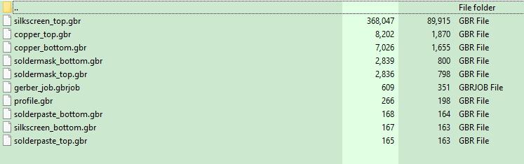
Download the HQDFM Gerber files for demo
The process of creating Gerber files typically begins after you complete a PCB (Printed Circuit Board) design, as a step to convert the design into a set of files that manufacturers can use to produce actual circuit boards. In most PCB design software, you will find an option to export or generate Gerber files. Here are some Gerber file export tutorials:
KiCad is easy to download, and it is free software that is applied for computer-aided design(CAD) and electronic design automation(EDA). This tool can help users realize their electrical circuits and create a BOM list, 3D view of the PCB + components, artwork, and Gerber files. Gerber file is the standard file type for PCB fabrication, PCB prototype, and PCB assembly. This article shows the steps on KiCad to Gerber file.
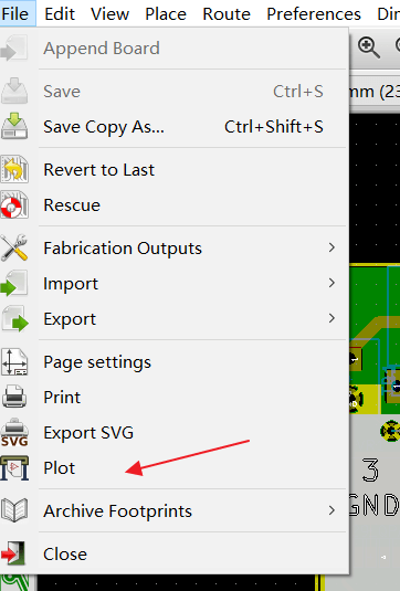
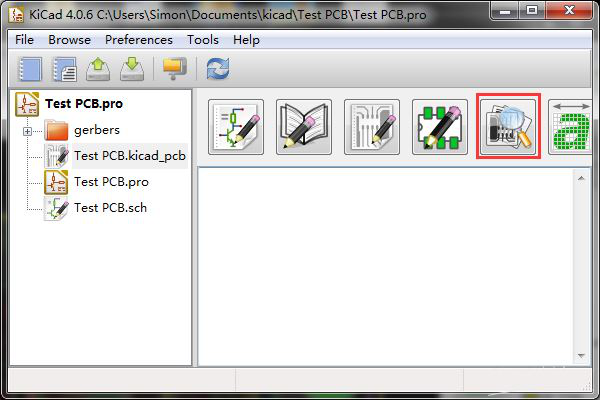
Step 1: Find the plot icon
Please find the PCB design file in KiCad and select "Plot" under the "Files" to open the Gerber generation tool.
Step 2: Plot settings
Select the layers and set an output directory for the Gerber files. Then click "Plot" to export the Gerber file for the layers.
NOTES: Please tick all layers if you are not sure which layers you need. NEXTPCB will help you to check the right layers for PCB manufacturing.
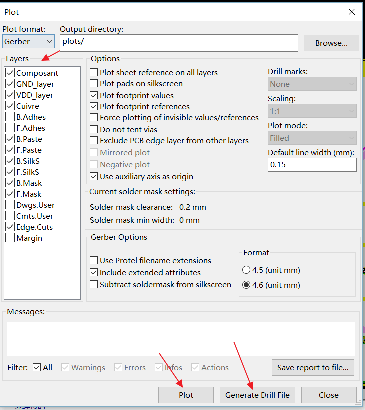
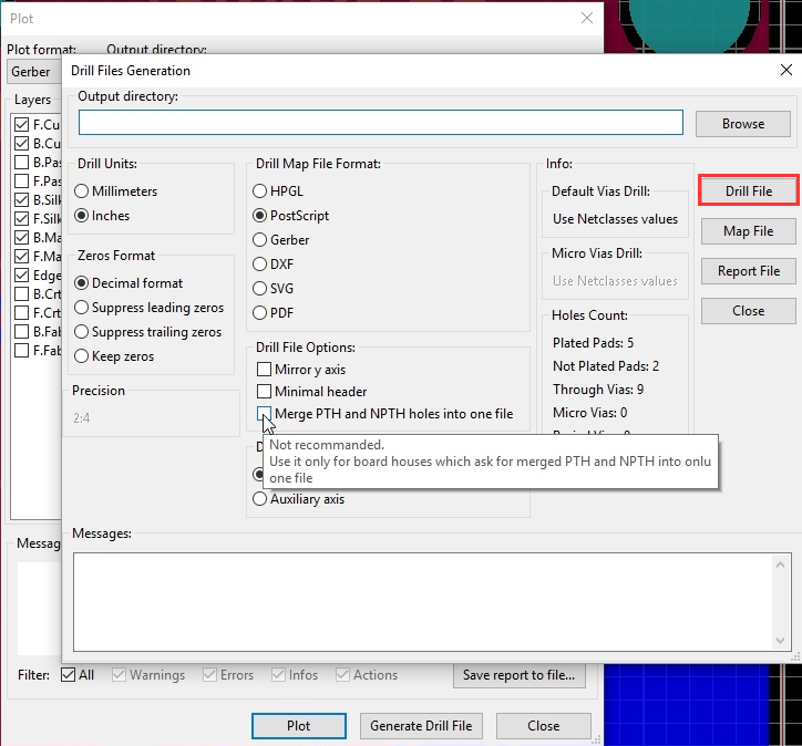
Step 3: Output Drill files
Ensure the Plot format is set to "Gerber." Next, please click the "Generate Drill File" button, and use the default values as the following picture. The output folder should be the default, which is the same as the Gerber files. Then click "Drill File" after everything is OK.
Step 4: Check the finished Gerber files
Please click "Close" to exit the windows of Plot and Drill. You can find all the data you need in the Gerber file folders. There is a Gerber viewer called "GerbView" in KiCad, and you can open it and check what the PCB looks like.
The Gerber files generated are all the production files PCB manufacturers need to quote and fabricate your PCBs. Please feel free to contact online services if you are still not clear about the processes.
If you need to place a PCB order on the NextPCB website, you should provide a Gerber file which is for PCB manufacturing. This article shows the steps on Altium to Gerber files.
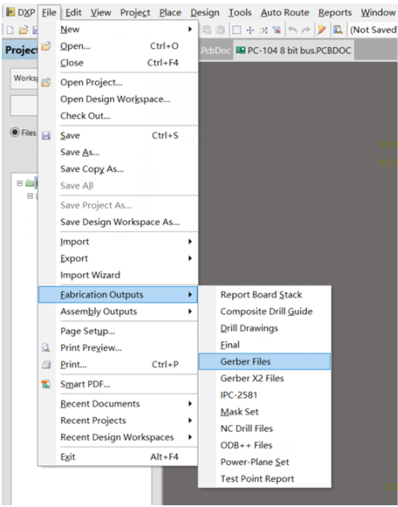
Step 1. Open you .PCBDOC design files on Altium designer software
Click: File -> Fabrication Outputs -> Gerber Files.
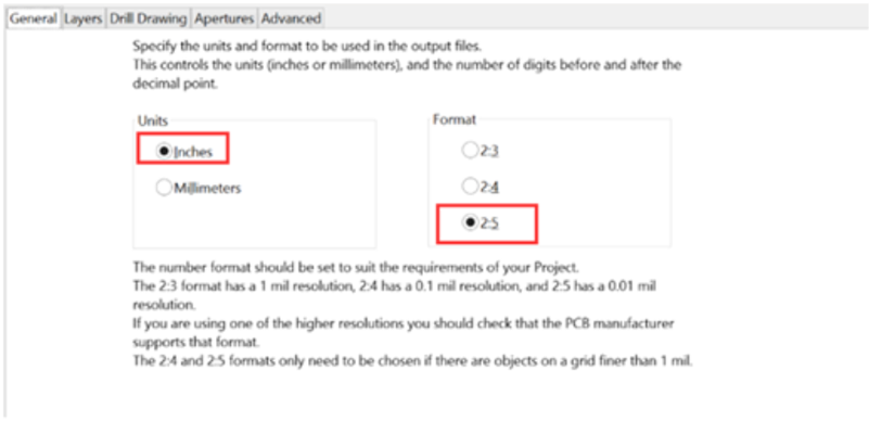
Step 2. General Setting
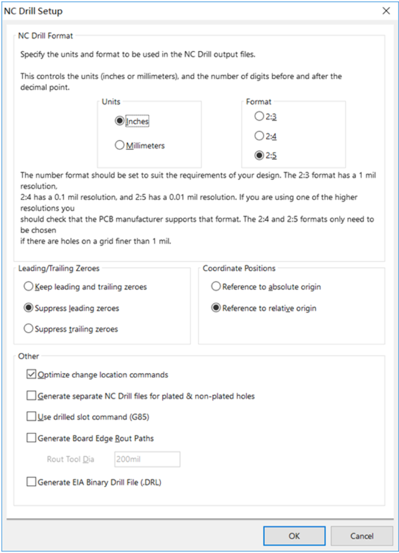
In the General Setting, please set the precision to 2:5 (0.01 mill resolution)
Step 3. Layers Setting
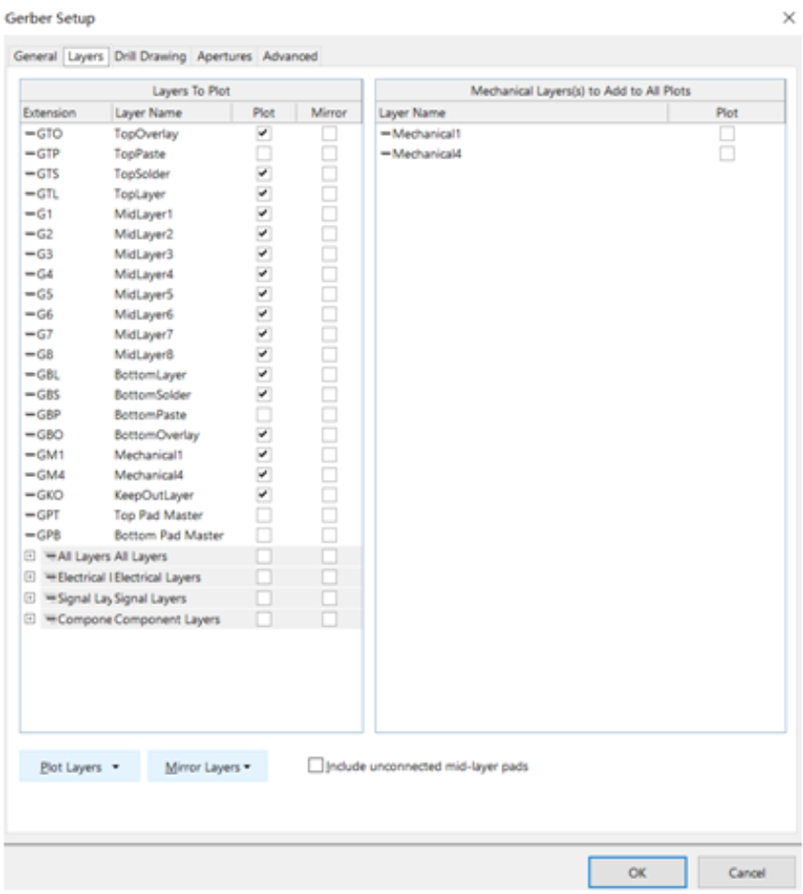
Firstly, please make sure you have a clear outline in the mechanical layer. If your board is a 2-layer PCB, there will be no inner layers (G1, G2, G3....). Include the layers that you want to export by marking these, select "Used On" in Plot Layers, and Select "All Off" in Mirror Layers.
Step 4. Aperture Setting
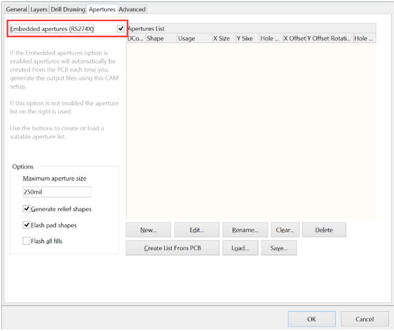
Please make sure to mark the "Embedded apertures (RS-274-X)" format.
Step 5. Advanced Setting
See the below picture, when you make sure all configurations are fine. Please click the "OK" to generate the Gerber files. Gerber Files will be automatically exported from the Altium cam viewer.
This tool allows you to verify that all layers have been generated correctly and that they are all in positive mode.

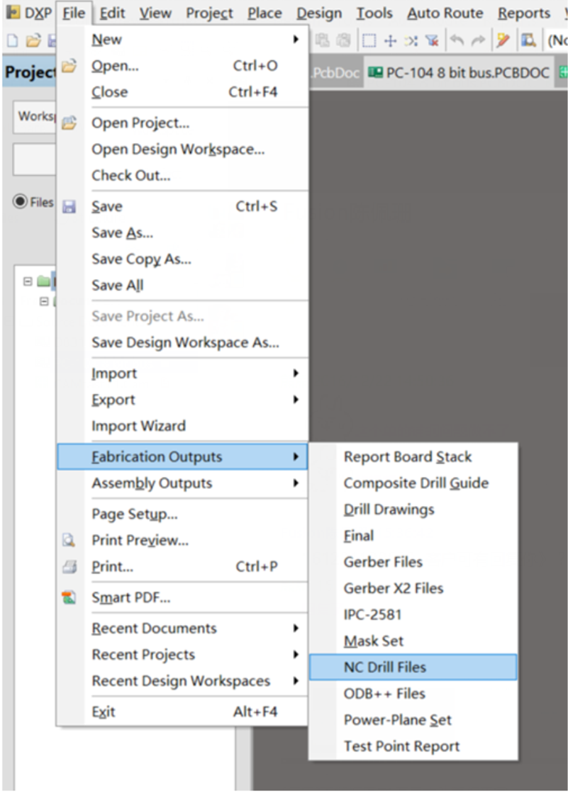
Step 6. Generating NC Drill Data
Don't forget to export the NC Drill data after generating the Gerber file. Many engineers will forget this step so that the supplier could not fabricate the PCBs without a drill data file.
a. Generate the Drilling layer in Excellon format.
Choose: File -> Fabrication Outputs -> NC Drill Files
b. We recommend you choose the same units and format parameters in this setting process for drill data. Then click "OK".
After this step, please zip the Gerber files and NC Drill data, and then the correct Gerber files have been done.
DipTrace is an EDA/CAD software for creating schematic diagrams and printed circuit boards. The developers provide a multi-lingual interface and tutorials (currently available in English and 21 other languages).
DipTrace has 4 modules: schematic capture editor, PCB layout editor with built-in shape-based autoroute and 3D-preview & export, component editor, and pattern editor. Comparing Altium and Eagle PCB design software, Diptrace software will be much easier to export Gerber files. This article shows the steps on Diptrace to Gerber file.
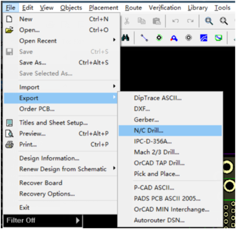
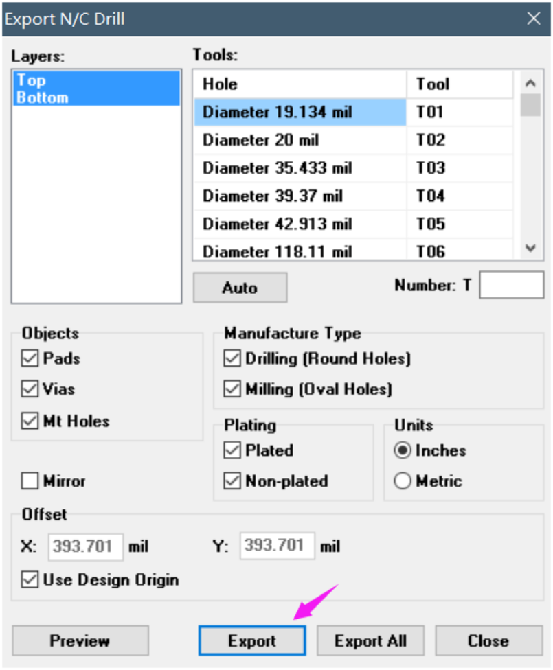
Step 1. Select File -> Export -> Gerber.
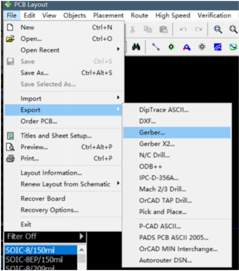
Step 2. Click "Export All" and save all the layers
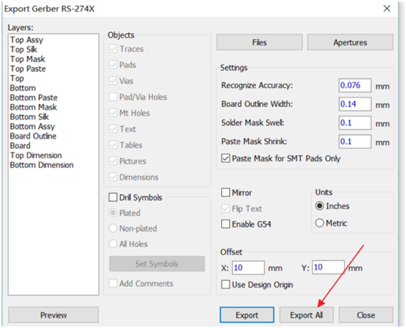
Step 3. After exporting the Gerber files, we need to export the NC Drill files.
This is the guide from NextPCB on how to Export Gerber files From Diptrace Software.
What is Eagle software?
EAGLE is a scriptable electronic design automation (EDA) application with schematic capture, printed circuit board (PCB) layout, auto-router, and computer-aided manufacturing (CAM) features. EAGLE stands for Easily Applicable Graphical Layout Editor (German: Einfach Anzuwendender Grafischer Layout-Editor) and is developed by CadSoft Computer GmbH. The company was acquired by Autodesk Inc. in 2016. EAGLE contains a schematic editor, for designing circuit diagrams. Schematics are stored in files.SCH extension, parts are defined in device libraries with LBR extension. Parts can be placed on many sheets and connected together through ports. The PCB layout editor stores board files with the extension.BRD. It allows back-annotation to the schematic and auto-routing to automatically connect traces based on the connections defined in the schematic. When you finish your PCB design in Eagle, you can generate Gerber files that are needed by the PCB manufacturer. This NextPCB article is telling you the steps Eagle to Gerber file.
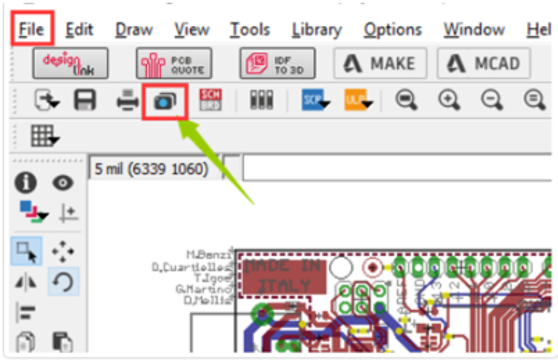
Step 1. Open the CAM Processor
Open your PCB layout (.brd) file in Eagle, Click the "CAM" button or choose "File -> CAM Processor". This will open the CAM Processor tool that is used to generate the files.
Step 2. Click File -> Open -> Job
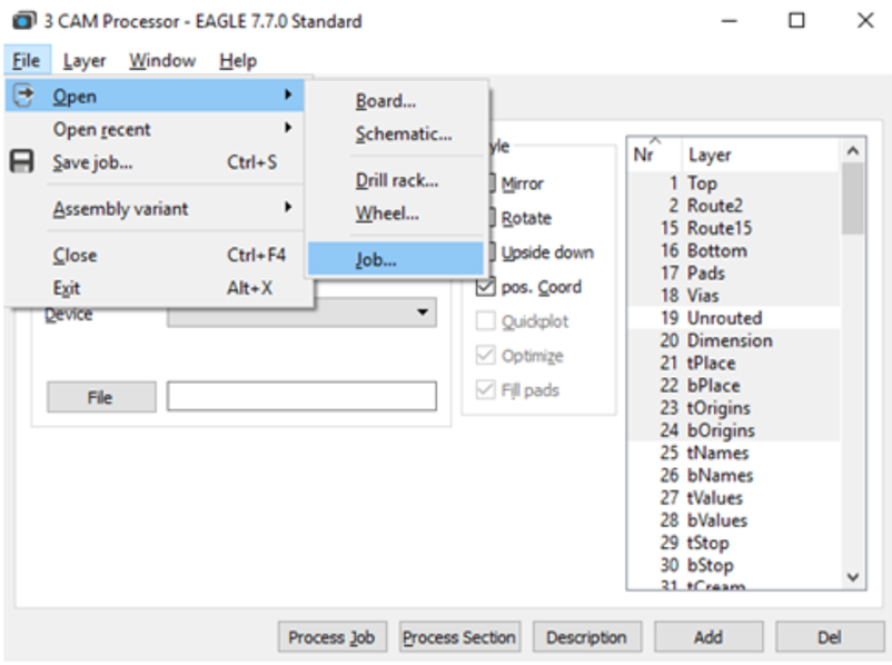
Step 3. Then navigate to your default EAGLE cam folder, choose the GERBER_RS274x.cam file, and press Open.
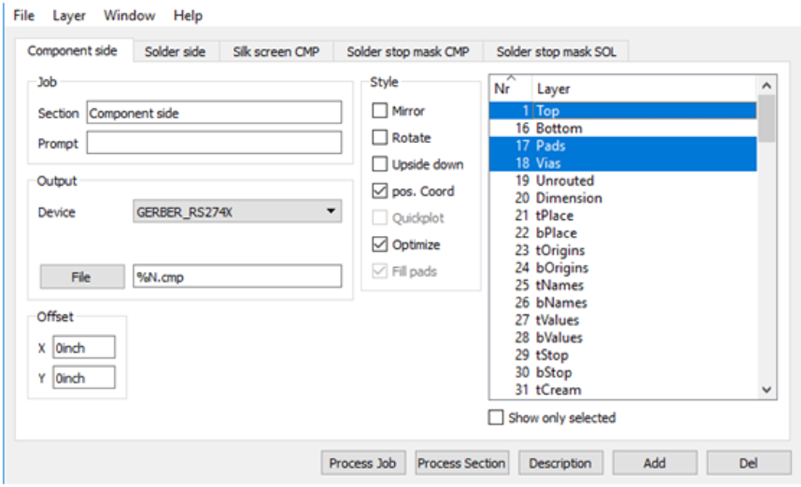
Step 4. Adding a second silkscreen (Optional)
If you look at the Layer options, it doesn't have a file for the silk screen bottom. But if you need a silkscreen on the bottom layer as well, follow these steps:
Step 5. Select the Process Job button to create all of your Gerber files.
You can find all of your generated Gerber files in the Autodesk EAGLEControl Panel in your project folder.
Step 6. Generating Your Drill File
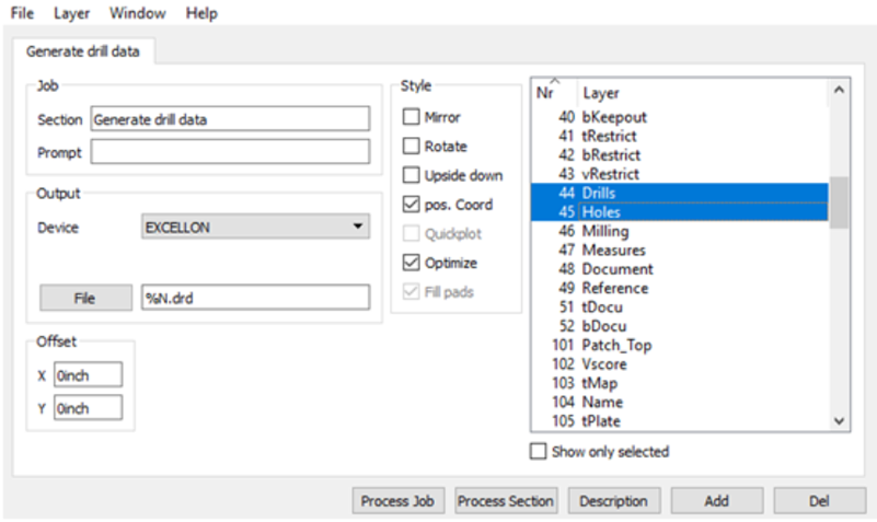
After those steps, Gerber files and Drill data have been exported from Eagle software.
Feel free to contact us: support@nextpcb.com if you have any more questions.
The fastest way to inspect your Gerber files before sending them to a PCB manufacturer
is to use a free online Gerber viewer — no software installation required.
NextPCB Free Online Gerber Viewer supports:
- RS-274X and Gerber X2 formats
- All PCB layers including copper, silkscreen, soldermask, and PCB drill files
- Layer toggle, zoom, and measurement tools
- DFM (Design for Manufacturability) checks
[→ Open Free Online Gerber Viewer]
To open Gerber files, you need to use specialized Gerber viewers or PCB design software. Here are some commonly used methods:
Furthermore, if you are in need of a free Gerber viewer, an excellent option is NextPCB's Free Gerber Viewer Online. NextPCB is a reputable PCB manufacturing and assembly service provider that offers a robust and user-friendly online Gerber Viewer tool. This free viewer allows you to open and inspect Gerber files seamlessly without the requirement of installing any software. It supports various Gerber formats, including RS-274X, Extended (X2) and OBD++, and provides a wide array of features such as zooming, rotation, measurement tools, and more, enabling you to conduct comprehensive analysis and verification of your PCB designs. Whether you are an experienced PCB designer or a novice, NextPCB's Free Gerber Viewer is a valuable resource that simplifies the process of viewing and examining Gerber files. What's more, it can analyze design defects online and generate DFM reports.
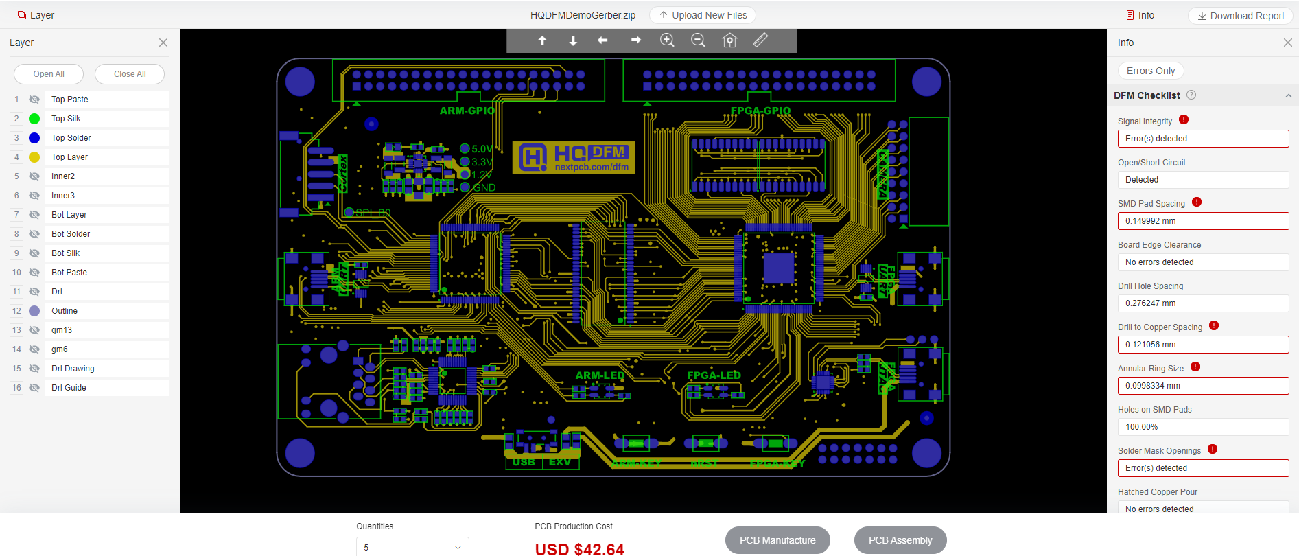
Check Your Gerber Files Online Now
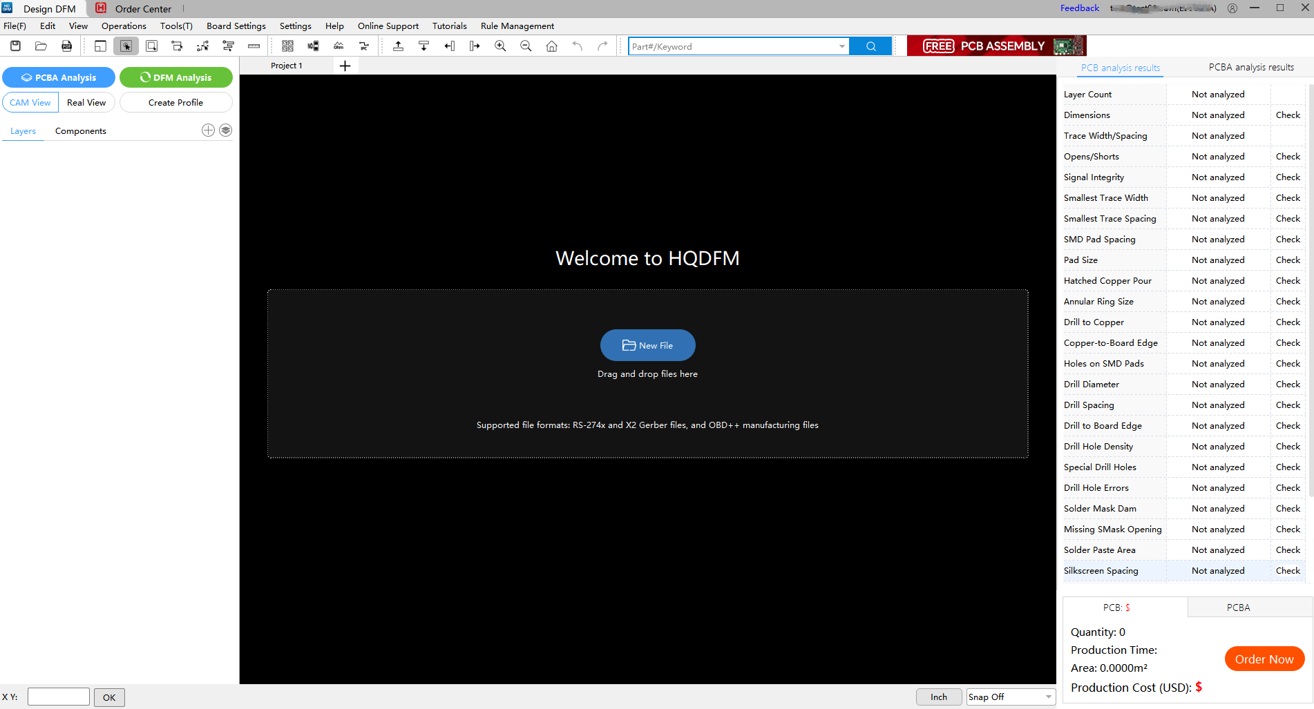
There is a comprehensive software solution that not only enables DFM and PCBA analysis but also There is a comprehensive software solution that not only enables DFM and PCBA analysis but also generates detailed DFM reports, offering the capability to export Gerber files as PDF.
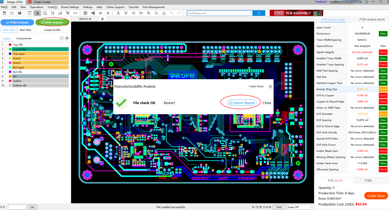
The HQDFM software incorporates powerful DFM analysis features, capable of detecting and identifying potential manufacturing issues such as inadequate component spacing, dense routing, pin conflicts, and more. By performing DFM analysis on Gerber files, HQDFM aids design engineers in identifying and resolving potential issues during the design phase, thereby enhancing design manufacturability and efficiency.
Moreover, HQDFM provides comprehensive PCBA analysis functionality, enabling the assessment of the feasibility and effectiveness of circuit board assembly. It automatically detects and evaluates aspects such as solder pads, component placement, silk screen markings, ensuring correct assembly and reliability of the circuit board.
In addition to complementing DFM and PCBA analysis, HQDFM generates detailed DFM reports. These reports encompass the results of DFM analysis and PCBA evaluation, along with recommended improvement measures. Through DFM reports, design engineers and manufacturers gain better insights into potential issues in the design and can take appropriate actions to enhance the manufacturing and assembly processes.
Furthermore, HQDFM includes the essential capability of converting Gerber files to PDF. This feature enables users to conveniently share and reference design files without the need for specific software or tools. PDF files offer broad compatibility and can be opened and viewed on various devices and operating systems.
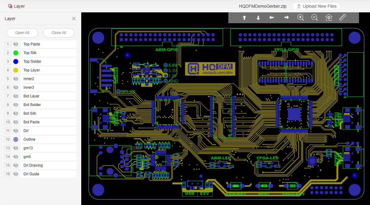
This is the main interface of HQDFM software:
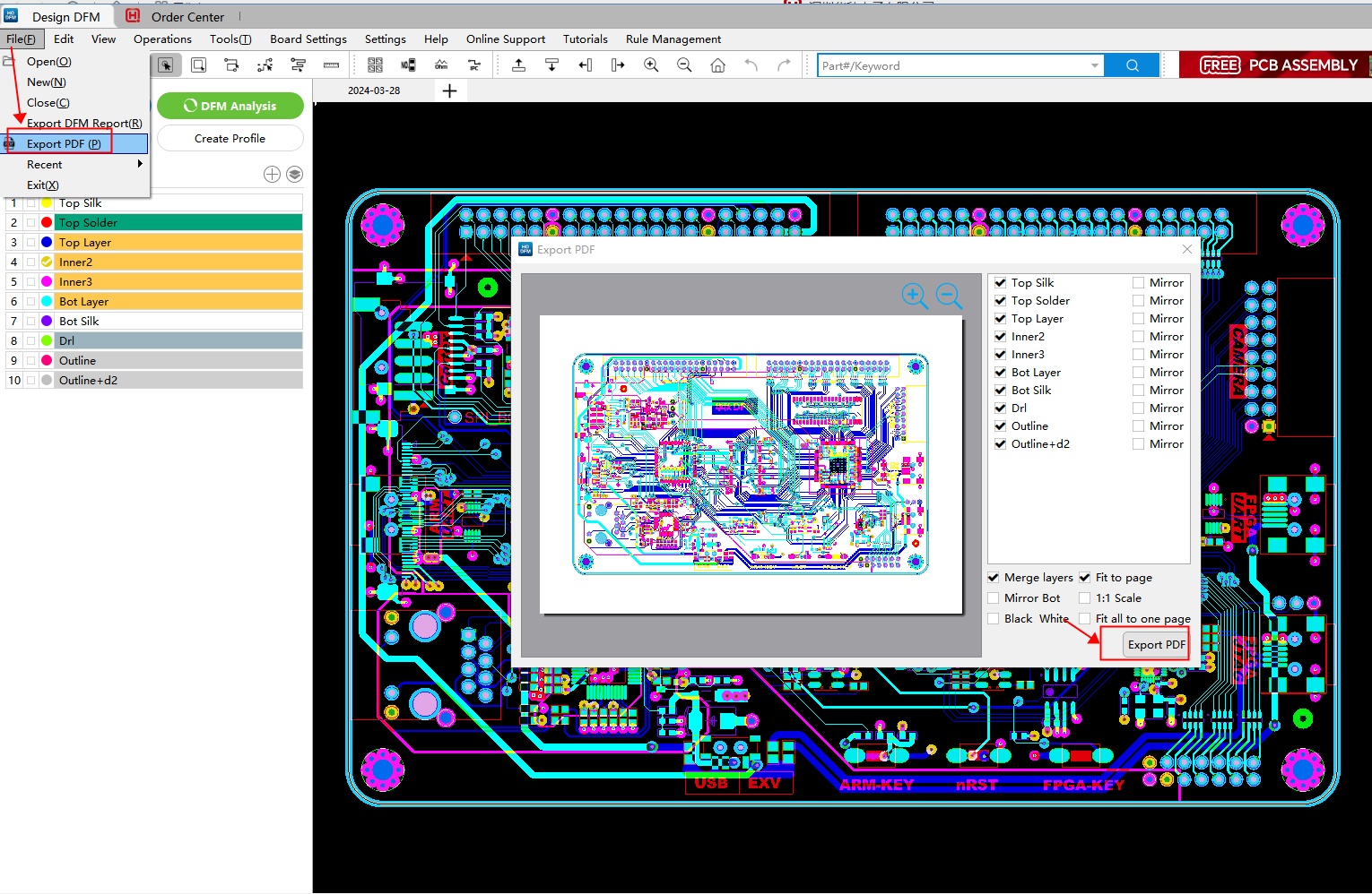
After uploading the Gerber file to the HQDFM software, click “File” in the upper left corner, and then select “Export PDF” to export gerber file to PDF.
Why not give HQDFM's DFM analysis and PCBA analysis features a try? It's completely free, giving it a shot and seeing how it works for yourself. Just like the demo file below, you can see that many errors were detected.
Converting Gerber files to PDF is useful for documentation, review, or sharing with
non-engineers. Here are the most common methods:
Method 1: Using HQDFM (Free)
1. Upload your Gerber files to HQDFM
2. Go to File → Export PDF
3. Select layers and export
Method 2: Using Altium Designer
1. Open Gerber files via File → Import
2. File → Smart PDF to generate PDF output
How to Convert Gerber to PNG
Use NextPCB's online viewer: upload Gerber → take screenshot, or use KiCad's
Plot function with SVG/PNG output option.
How to Convert Gerber to STEP
STEP conversion requires PCB design software (Altium, KiCad).
KiCad: File → Export → STEP.
Gerber files play a crucial role in the manufacturing of printed circuit boards (PCBs) within the PCB industry. Gerber files serve as the standard format for describing PCB designs and encompass information regarding component placement, routing, pads, silkscreen, and other design elements.
In the PCB manufacturing process, manufacturers rely on Gerber files to perform a series of operations that transform the design into an actual PCB.
Manufacturers typically need the original Gerber files for adjustments and optimization. For example, if your original design has a line width of 6mil, but the file you send to the supplier shows a width of 6.6mil, this modified file is referred to as a "working Gerber" (used for production). Such files have been processed through CAM, potentially including manufacturing compensation, process optimization, and other necessary adjustments. Given that each manufacturer has its own engineering workflow, they may find these changes unclear.
In summary, Gerber files serve as a bridge and guide within PCB manufacturing, transforming design engineers' creativity into tangible PCBs. Manufacturers rely on Gerber files for process preparation, layer generation, manufacturing process control, and quality inspection to ensure that the produced PCBs align with the design and meet quality standards.
Ensuring the completeness and accuracy of Gerber files for pcb is crucial for guaranteeing that each pcb board meets the required specifications when it is produced. Here are some of the most common Gerber file issues encountered by HQNextPCB, a PCB manufacturer with over 15 years of production experience, and what can be done to address them:
Among all the potential issues your PCB might encounter, Gerber file errors are the least forgivable. While most PCB design errors can be avoided with more careful and focused work, Gerber file errors are the easiest to prevent. Given that the consequences of Gerber file issues can be expensive and time-consuming, you simply cannot afford to let them occur. How to avoid Gerber file issues? Here are some methods to help you:
By implementing these measures, you can significantly reduce the risk of Gerber file issues and ensure a smoother, more efficient PCB production process.
Check Your Gerber Files Online for Free
In project development, time is critical – and NextPCB delivers. We're your one-stop solution for PCB manufacturing and assembly, turning your designs into reality with speed and precision. From high-quality bare boards to advanced PCB Assembly, NextPCB handles both prototypes and mass production. Our expert DFM support ensures top-tier quality and efficiency. Partner with us to streamline your supply chain and accelerate your projects with reliable, trusted PCB solutions.
Gute Nachrichten: Die deutschsprachige Version des Gerber Viewer ist jetzt online! Kostenloses Online-Gerber-Viewer
Ready to verify your Gerber files?
→ Use NextPCB's Free Online Gerber Viewer — check all layers, run DFM analysis, and get instant manufacturing feedback. No download needed. [View Your Gerber Files Free →]
A: In KiCad, open your PCB layout, go to File → Plot, select "Gerber" as the output format,
choose your layers, and click "Plot." Then click "Generate Drill File" for the drill data.
Zip all files before submitting to your PCB manufacturer.
A: RS-274X (Extended Gerber) is the industry standard that embeds aperture definitions
within the file. Gerber X2 is the newer format that adds metadata such as layer
function, material info, and component data — making it more information-rich for
automated manufacturing workflows.
A: Upload your Gerber files to HQDFM (free online tool), then use File → Export PDF.
Alternatively, open Gerber files in KiCad and use File → Print to PDF.
Still, need help? Contact Us: support@nextpcb.com
Need a PCB or PCBA quote? Quote now


 Surface

