
 Surface


Stacy Lu

 NextPCB Capabilities
Printed Circuit Boards
NextPCB Capabilities
Printed Circuit Boards
 PCB Assembly
 Layer Buildup
 SMD-Stencils
 PCB Design-Aid & Layout
 Mechanics
 Quality
 Drills & Throughplating
 Factory & Certificate
 PCB Assembly Factory Show
Certificate
PCB Assembly Factory Show
Certificate
Support Team
Feedback:
support@nextpcb.com


Introduction
For those in the electronics industry, it's well known that chip packaging is akin to dressing the intricate "electronic brain" in a protective outer layer. This "coat" not only safeguards the delicate silicon chip but also plays a critical role in enabling communication with the outside world. Today, let's explore the nine most common chip packaging technologies on the market and delve into the ingenious designs within these compact forms.
In short: IC packaging is the process of enclosing a semiconductor chip in a protective case with external leads, pads, or balls that connect it electrically and mechanically to a PCB. There are hundreds of IC package variants in total, but this guide covers the 9 most common types used in modern electronics today: DIP, QFN, DFN, PLCC, the SOP family, LQFP, BGA, WLCSP, and PGA.
Last reviewed: [MONTH YEAR] | Reviewed by the NextPCB engineering content team
Table of Contents
Dual In-line Package (DIP) has been a mainstay in the electronics world since its inception in 1965. This black, rectangular package with metal pins on both sides was the standard for 1980s electronics. While it has gradually been replaced by Surface-Mounted Device (SMD) packages, DIP still holds its ground in certain applications.
DIP packaging is simple and widely used for small to medium-scale integrated circuits (ICs). CPUs with DIP packaging typically have two rows of pins (usually no more than 100), making them easy to insert into DIP-compatible sockets or directly solder onto a circuit board. Common applications include standard logic ICs, memory LSI, and microelectronic circuits.
Despite the demand for smaller electronics, DIP's larger pin spacing (typically 2.54mm) means it remains bulky but is still prevalent in industrial control devices, experimental circuit boards, and even vintage equipment. Recently, while repairing an old amplifier, I discovered DIP packaging in its power module. Though it is gradually being overshadowed by more compact and efficient packaging forms, DIP remains a key part of the electronics industry.
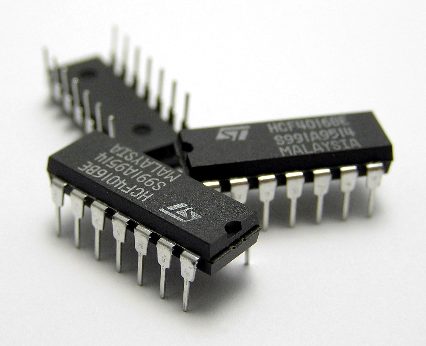
image from wikipedia Dual_in-line_package
The Shrink Dual In-line Package (SDIP), also known as Narrow Pitch Dual In-line Package or Compressed Dual In-line Package, is a type of through-hole package. SDIP is a derivative of the DIP package, having the same shape as the DIP but with a smaller lead pitch (1.778mm) compared to DIP (2.54mm). The number of leads ranges from 14 to 90, and the materials used can be either ceramic or plastic.
> Recommend reading: A Guide to Through-Hole Assembly Technology
When talking about the most popular packaging technologies today, Quad Flat No-lead (QFN) packaging definitely ranks among the top three. This leadless square package connects through pads on the bottom, almost like putting an invisible armor on the chip. The QFN package has a large exposed pad at the center of the bottom, which effectively dissipates heat, while the surrounding pads are for electrical connections. When disassembling a flagship smartphone from a certain brand, it was found that the main control chip uses a 0.4mm pitch QFN-48 package, with its secret weapon being the central exposed pad, which not only allows for fast heat dissipation but also enhances the structural strength of the package.
Unlike traditional SOIC and TSOP packages, QFN does not have gull-wing leads. The conductive path between the internal pins and pads is short, greatly reducing the self-inductance and the resistance of the internal wiring, thereby offering excellent electrical performance. In addition, QFN further improves thermal performance through the exposed lead frame pads on the bottom, which are connected to heat dissipation pads and vias on the PCB. This effectively spreads the excess heat, helping the chip maintain a stable operating temperature.
However, despite QFN's excellent electrical performance and heat dissipation capabilities, beginners need to be cautious when soldering. Particularly with the surrounding pads, there is a tendency for cold solder joints, and precise control of the reflow soldering temperature profile is required to ensure soldering quality.
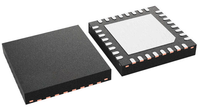
Quad Flat No-lead (QFN) packaging definitely ranks among the top three most popular packaging technologies today. This leadless square package connects through pads on the bottom. Crucially, the QFN package features a large exposed pad at the center of the bottom, which functions primarily as a heat sink pad. This exposed pad effectively dissipates heat, while the surrounding pads are for electrical connections.
Unlike traditional SOIC and TSOP packages, QFN does not have gull-wing leads. The conductive path between the internal pins and pads is short, greatly reducing the self-inductance and the resistance of the internal wiring, thereby offering excellent electrical performance. The exposed lead frame pads on the bottom, connected to heat dissipation pads and vias on the PCB, further improve thermal performance, helping the chip maintain a stable operating temperature.
However, despite QFN's excellent electrical performance and heat dissipation capabilities, beginners need to be cautious when soldering. Particularly with the surrounding pads, there is a tendency for cold solder joints, and precise control of the reflow soldering temperature profile is required to ensure soldering quality. It is important to note that the soldering quality of QFN is easily affected by factors such as the temperature profile, solder paste type, and PCB design, especially during reflow soldering.
Quick view:
| Advantages | Disadvantages |
| Excellent Electrical Performance: Shorter conductive paths, improved electrical efficiency (inductance and capacitance improved by 60% and 30%). | Soldering Difficulty: Solder points are located at the bottom, making visual inspection difficult. |
| Superior Thermal Performance: Large exposed heat sink pad and shorter internal path (55% better than TSSOP). | Complex Rework: Soldering defects (bridging, open circuits) make the repair process complicated. |
| Compact Size and Light Weight: Dimensions reduced by 62% compared to TSSOP, suitable for high-density assembly. | Cold Solder Joints: A tendency for cold solder joints with the surrounding pads, requiring strict control over the reflow process. |
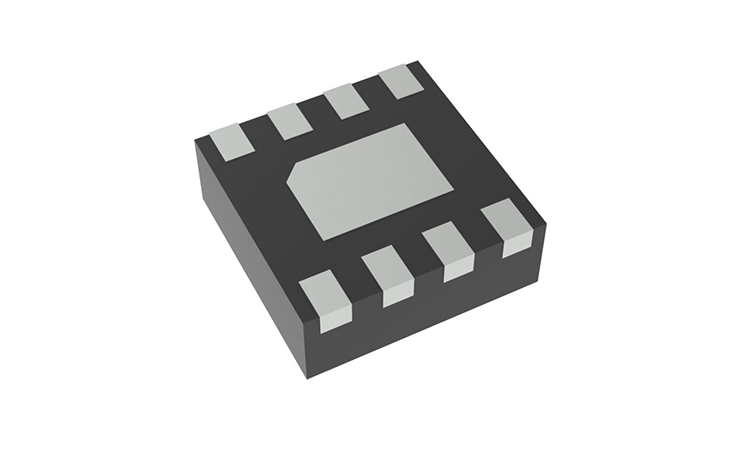
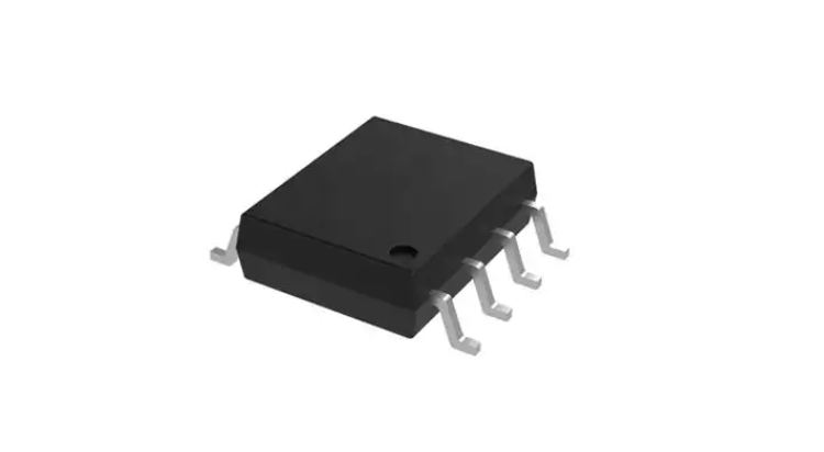
Dual Flat No-lead (DFN) packaging is a leadless, flat packaging form that is typically square or rectangular in shape. Similar to QFN, DFN features large exposed pads on the bottom for heat dissipation, surrounded by electrical connection pads. Unlike QFN, DFN typically only has pads on two sides.
The structure shortens the conductive path, reducing inductance and trace resistance, which improves electrical performance and signal integrity. The most prominent feature of DFN packaging is its compact size, with the smallest dimensions reaching as small as 2×2mm, making it even slimmer than QFN. Due to its minimal footprint and low profile, DFN is the preferred choice for applications where board space is severely limited.
Typical Application: Portable electronic products such as smartwatches and Bluetooth earphones, low-power consumption sensors, wireless communication modules, and pressure sensors in blood glucose meter projects.
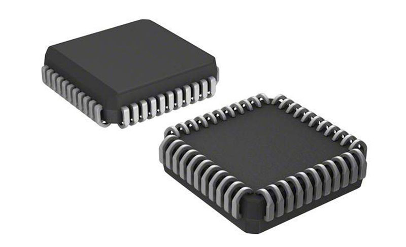
Plastic Leaded Chip Carrier (PLCC) packaging is a traditional integrated circuit packaging form, typically square or rectangular, smaller than DIP packaging, and offers higher reliability. It uses surface-mount technology (SMT) and features gull-wing leads extending from all four sides, which enables efficient installation and wiring on the PCB. PLCC packaging is widely used in various electronic devices such as computers, communication equipment, and consumer electronics, particularly in applications that require high mechanical strength and electrical performance.
Although it was once thought that PLCC would be replaced by more advanced packaging technologies, it has found new life in the LED display industry. Its unique gull-wing lead design effectively alleviates thermal stress, making it particularly suitable for applications that involve frequent temperature changes. An industrial display manufacturer has stated that they continue to use PLCC packaging for their LED driver chips because the failure rate is 30% lower than with QFN packaging.
However, when using PLCC packaging, it's important to note that socket connections can suffer from poor contact, making direct soldering a more reliable option. Despite this, PLCC packaging still maintains a strong position in certain fields due to its compact size, excellent thermal management capabilities, and good mechanical strength, representing a comeback for the "veteran" technology in the electronics industry.
PLCC Packaging is still adopted by many industrial and commercial applications due to its robust mechanical strength and proven thermal management capabilities.
Advantages:
Disadvantages:
Typical Application: Computers, communication equipment, consumer electronics, and particularly in industrial control devices, automotive systems, and LED display drivers that require high mechanical strength and thermal stability.
> For further details on PLCC packaging, please refer to "PLCC Packages: A Comprehensive Guide Is Here"
From the standard Small Outline Package (SOP) to the Thin Shrink Small Outline Package (TSSOP), this family perfectly demonstrates the concept of "small size, big energy." A recent IoT terminal design utilized an SSOP-20 packaged RF chip, which integrates complete wireless functionality within an area of 10 × 5.3mm.
SOP packaging is characterized by its small size, light weight, and high packaging density. It is widely used in memory chips, amplifiers, and various other functional blocks. The SOP family of packages is typically mounted on the circuit board using Surface Mount Technology (SMT). Its pins extend in an L-shape or gull-wing form from the sides of the package, with small pin spacing, allowing for more pins and supporting more complex circuit designs.
LQFP (Low-profile Quad Flat Package) is an integrated circuit packaging form that utilizes surface-mount technology (SMT). Its distinctive feature is the flat leads on all four sides, with the leads extending from the package in a “gull-wing” shape, which facilitates soldering and inspection. LQFP packages typically have a thickness of 1.4mm or thinner, making them ideal for space-constrained applications. Common lead pitches are 0.5mm, 0.65mm, or 0.8mm, and the number of pins ranges from 32 to 256, with applications commonly found in the range of 64 to 144 pins.
LQFP packaging is widely used in microcontrollers (MCUs), communication chips, and consumer electronics, particularly in the mid-range chip market that requires numerous I/O ports. LQFP has always held a prominent position in this segment. An engineer from an MCU manufacturer revealed that adopting LQFP-100 packaging can effectively reduce production costs by up to 15%. However, while the thin profile offers the advantage of compact size, it also requires high precision in placement, and special attention must be paid to PCB deformation during production to ensure precise installation of the package.
Despite its low cost and broad applicability, LQFP packaging has relatively poor heat dissipation performance. In high-power applications, additional cooling measures may be necessary. Additionally, in practice, the corner solder pads of LQFP chips are most susceptible to cold solder joints. Therefore, special attention must be paid during production to inspect and ensure the quality of soldering.
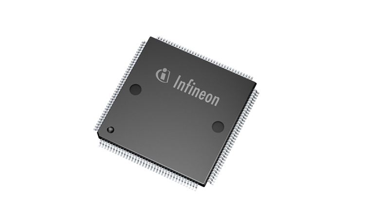
Image sourcing: infineon
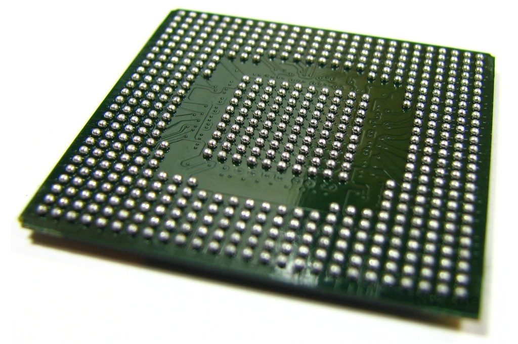
When the number of pins exceeds 300, Ball Grid Array (BGA) packaging becomes the only choice. BGA is an SMT technology that connects the chip to the PCB using solder balls for signal transmission. Compared to traditional QFP (Quad Flat Package), BGA packaging has higher I/O (input/output) density and experiences less stress caused by thermal expansion coefficient differences, which improves the stability and reliability of the device.
For example, in a gaming graphics card project, the GPU chip uses a 1156-ball BGA package, and its soldering yield directly determines the success or failure of the high-end product. For small batch production in the R&D stage, it is recommended to use reworkable BGA packages with ball placement to allow for repairs when issues arise. However, it is important to note that BGA rework must be done using X-ray inspection, as it is difficult to detect fine shorts between solder balls with the naked eye.
X-ray inspection is commonly used to examine BGA solder joints, particularly in high-density applications, where it is crucial for ensuring there are no hidden issues like shorts, bridging, or insufficient solder volume beneath the package. For complex high-pin-count packages, X-ray inspection is key to ensuring soldering quality.
Quick view:
| Advantages | Disadvantages |
| High Yield: Significantly reduces solder joint failure rate compared to narrow-pitch QFP. | Non-Ductile Connections: Solder balls lack ductility, which can cause breaks under thermal or mechanical stress (can be addressed by bottom-fill materials). |
| Superior Electrical Performance: Shorter leads greatly enhance electrical performance, providing stable signal transmission. | Inspection Difficulties: Solder joints are at the bottom; requires X-ray or other advanced equipment for inspection. |
| High Pin Density: Allows for more pin connections within a smaller chip size. | Complex Development Rework: Soldering is complex and requires specialized equipment; manual soldering has lower reliability. |
| Improved Heat Dissipation: Thermal performance improved through exposed solder pads at the bottom. | Cost: Rework and inspection complexity adds to the overall cost. |
> Recommend reading: LGA vs BGA: Which One is Right for You?
Although BGA packaging technology demonstrates significant advantages such as high yield, superior electrical performance, high pin density, reliability, good heat dissipation, and suitability for high-density packaging, it is not without challenges.
BGA packaging comes in several different types, each with its own advantages and suitable applications:
Each type of BGA packaging has different strengths and is suited for specific application scenarios. Designers can choose the appropriate package type based on their specific needs to meet the chip's performance, cost, and reliability requirements.
For further details on BGA packaging types, please refer to "7 Types of BGA (Ball Grid Array) Packages"
Wafer-Level Chip Scale Packaging (WLCSP) is a disruptive technology in the semiconductor packaging field that is rapidly transforming the industry landscape. WLCSP technology eliminates the steps of cutting and testing associated with traditional packaging methods by performing packaging and testing directly on the entire wafer, resulting in a package size almost identical to the original chip. This innovation has led to an extreme miniaturization effect. For example, the latest 5G module from a leading mobile chip manufacturer, after adopting WLCSP packaging, has reduced its size by 60%, and the thickness of the chip can be as thin as 0.6mm. For applications with strict space requirements, such as smartphones and wearable devices, WLCSP undoubtedly provides an ideal solution.
Compared to traditional packaging methods, WLCSP significantly reduces the volume and cost by eliminating extra steps in the packaging process. For applications with strict space requirements, such as smartphones and wearable devices, WLCSP undoubtedly provides an ideal solution due to its ultra-small size and excellent electrical performance.
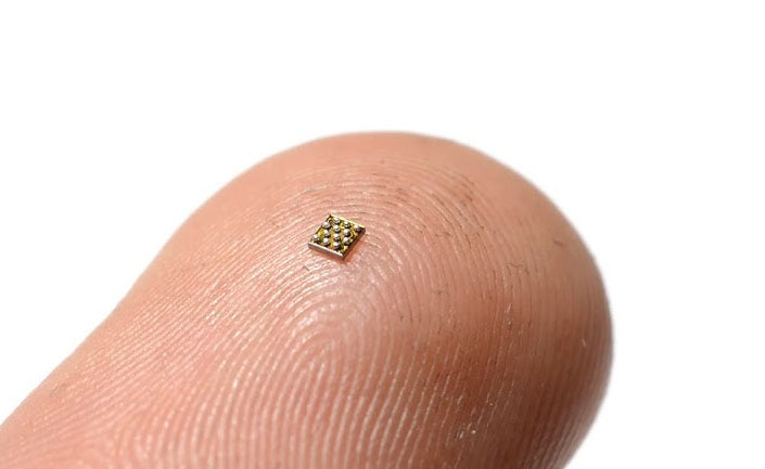
Image sourcing: internet
Quick view:
| Advantages | Challenges |
| Minimal Size: Package volume is approximately equal to the bare chip size, suitable for space-sensitive applications such as smartphones and wearable devices. | Thermal Limitations: The small size leads to insufficient heat dissipation area, requiring additional thermal design for high-power chips. |
| Optimized Electrical Performance: The short signal paths reduce inductance and resistance, enhancing high-frequency performance, making it suitable for RF (5G/Wi-Fi) and high-speed chips. | Lower Mechanical Strength: The lack of traditional packaging protection may require bottom-filling adhesives to enhance impact and thermal cycling resistance. |
| Cost Efficiency: Wafer-level batch processing reduces the cost per chip, especially in large-scale production, by simplifying the supply chain. | Limited I/O Count: The solder ball layout is constrained by the chip's area, making it suitable for chips with medium-to-low pin counts. |
| Simplified Supply Chain: The integration of packaging and manufacturing processes reduces intermediate steps. |
WLCSP stands out for its extreme miniaturization and high performance. Despite challenges in heat dissipation and mechanical strength, its advantages in mobile communication, IoT, and other fields make it an important choice for modern semiconductor packaging. With ongoing advancements in 3D integration, advanced materials, and other technologies, the application scope of WLCSP is expected to expand further.
Pin Grid Array (PGA) packaging is an integrated circuit (IC) packaging technology commonly used for microprocessor packaging. In PGA packaging, the integrated circuit (IC) is placed inside a ceramic package, and the bottom of the ceramic is designed with an array of pins arranged in a square pattern. These pins can be inserted or soldered into corresponding sockets on the circuit board. This unique pin connection method makes PGA packaging particularly suitable for applications that require frequent insertion and removal.
The key feature of PGA packaging lies in the design of its pins. Each pin is vertical to the circuit board (PCB), providing stable electrical connections and high pin density, making it ideal for processors requiring a large number of I/O connections. However, this design also introduces some challenges. Since the pins in PGA packaging are relatively long and prone to damage, careful handling is required during installation or removal. If the heatsink is installed too tightly, it may cause the CPU to come off with the heatsink or damage the pins. To avoid this risk, PGA packaging typically uses a side clamp method to secure the components.
Despite some drawbacks, such as less stability during installation—especially in AMD’s socket design, where the CPU may come off with the heatsink during disassembly—PGA still demonstrates certain advantages. For instance, because the pins in PGA packaging are vertically designed, if a pin bends, it is relatively easy to restore manually. In contrast, LGA packaging features more complex pin designs that are much harder to fix, making recovery largely dependent on luck.
PGA packaging is widely used in AMD desktop CPUs and other products. It offers high packaging strength and durability, making it suitable for frequent insertion, removal, and overclocking operations. Compared to other packaging types, PGA packaging is better able to withstand environments with frequent hardware adjustments, reducing the risk of hardware failure caused by packaging issues.
In conclusion, PGA packaging, as a classic connection method, still holds an important place in high-density and high-performance applications. While its usage has decreased with the rise of LGA packaging, it continues to play a significant role in certain specific areas.
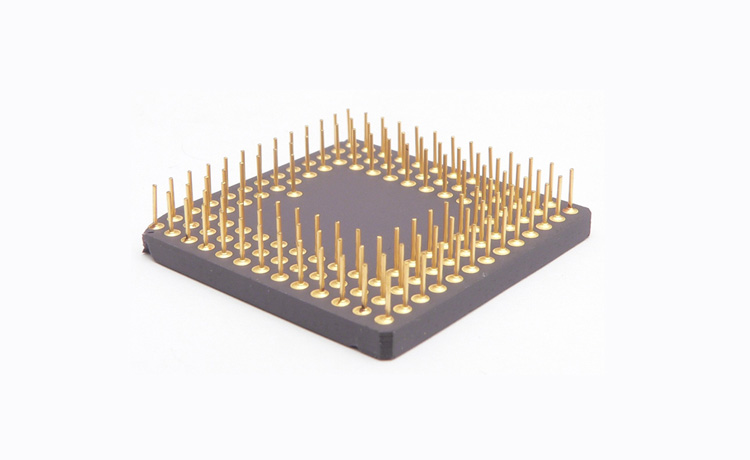
image from wikipedia Pin Grid Array Packaging
PGA packaging is suitable for situations that require frequent insertion and removal, such as microprocessors, image processors, and FPGAs, among other high-performance integrated circuits.
The application fields of PGA packaging are very extensive, mainly including the following aspects:
Overall, PGA packaging excels in high density, high performance, good heat dissipation, and reliability, making it an ideal packaging choice for many high-end electronic applications.
Although PGA packaging is gradually being replaced by BGA and LGA, it still holds significant importance in certain fields due to its good maintainability and flexibility.
If you don't have a datasheet handy, you can usually identify a package type in three steps: (1) check whether it mounts through-hole or on the surface, (2) look at the lead/contact style around or under the package, and (3) measure the lead pitch and pin count. The table below maps each of the 9 package types above to these identification cues.
| Package | Mounting | Lead/Contact Style | Typical Giveaway |
| DIP | Through-hole | Two rows of straight metal pins | 2.54mm pin spacing, black rectangular body |
| QFN | SMT | No leads — flat pads on the underside only | Large exposed thermal pad in the center of the bottom |
| DFN | SMT | No leads, pads on 2 sides only (vs. QFN's 4 sides) | Very small footprint, down to 2×2mm |
| PLCC | SMT (or socketed) | Gull-wing leads on all 4 sides | Square/rectangular, often seen in a socket |
| SOP family | SMT | L-shape or gull-wing leads on 2 sides | Small, narrow-body IC; TSOP/SSOP/VSOP variants differ mainly in thinness/pitch |
| LQFP | SMT | Gull-wing leads on all 4 sides | Thin (≤1.4mm) square body, 32-256 pins |
| BGA | SMT | Solder balls on the underside | No visible leads at all; used once pin count exceeds ~300 |
| WLCSP | SMT | Solder balls, package roughly the size of the bare die | Package size is nearly identical to the silicon chip itself |
| PGA | Socketed (pins inserted) | Grid array of pins on the underside | Ceramic body, pins perpendicular to the board, common on desktop CPUs |
When the markings are unclear or a package has been reworked, the same identification methods used in production — X-ray inspection for ball/hidden-lead packages like BGA and WLCSP, and visual/optical inspection for leaded packages — can confirm what you're looking at.
What is IC packaging?
IC packaging is the process of enclosing a semiconductor chip in a protective case with external leads, pads, or solder balls that connect it electrically and mechanically to a PCB, while also protecting it from moisture, heat, and mechanical stress.
How many types of IC packaging are there?
There are hundreds of IC package variants in total, but the 9 most common types used in modern electronics are DIP, QFN, DFN, PLCC, the SOP family (SOP/TSOP/SSOP/VSOP), LQFP, BGA, WLCSP, and PGA.
What is the most common IC package type today?
QFN and BGA are among the most widely used package types in current consumer electronics — QFN for its compact, leadless design in mobile devices, and BGA for high-pin-count chips such as CPUs and GPUs that need very high I/O density.
How do you identify an IC package type without a datasheet?
Check the mounting style (through-hole vs. surface-mount), the lead or contact style (gull-wing leads, no-lead pads, solder balls, or pins), and the lead pitch/pin count. See the identification table above for how each of the 9 common package types differs on these three points.
What's the difference between through-hole and surface-mount IC packages?
Through-hole packages, such as DIP and PGA, have pins that insert into holes drilled through the PCB and are soldered on the opposite side. Surface-mount packages, such as QFN, DFN, PLCC, the SOP family, LQFP, BGA, and WLCSP, are soldered directly onto pads on the board surface, allowing for smaller size and higher-density assembly.
The evolution of packaging technology is like a miniature history of electronic development: from DIP to WLCSP, packaging volume has decreased by 95%, while performance has increased by thousands of times. Choosing a packaging solution should not be about blindly chasing trends, but rather about comprehensively considering factors such as cost, process, and reliability. For example, QFN is sufficient for smart home products, while aerospace equipment may still require the proven PLCC packaging. When designing circuits next time, it might be helpful to communicate more with packaging engineers and reliable pcb manufacturers; you may find unexpected optimization solutions. After all, a good package is not just a protective shell but also a performance booster.
Are you ready to optimize your next electronic design?
Understanding the nuances of chip packaging can be the key to unlocking better performance, lower costs, and improved reliability for your product. Don't let your "electronic brain" wear the wrong coat!

Still, need help? Contact Us: support@nextpcb.com
Need a PCB or PCBA quote? Quote now

