Blog / PCB vs PCBA: The Critical Distinction Electronics Creators Must Master
PCB vs PCBA: The Critical Distinction Electronics Creators Must Master
Posted: October, 2024Last Updated: May, 2026Writer: Robin
Share:
Introduction
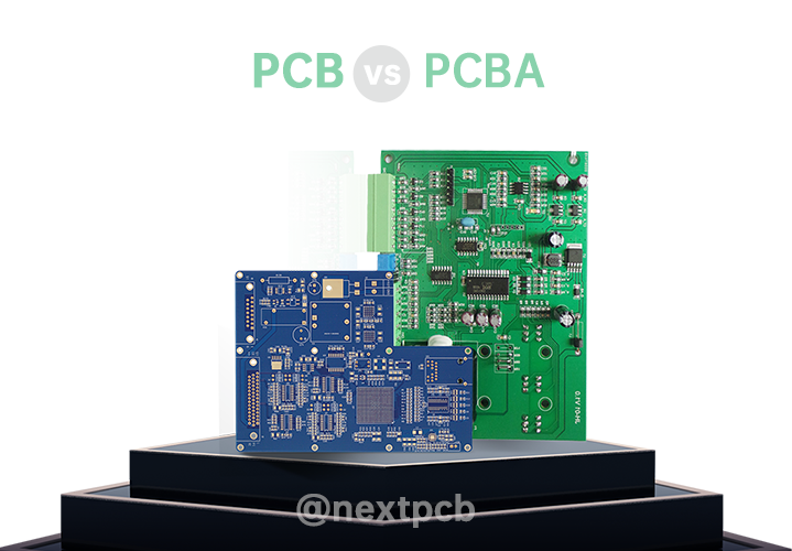
When you're diving into electronics, you'll often come across the terms PCB (Printed Circuit Board) and PCBA (Printed Circuit Board Assembly). While they sound similar, they actually refer to two different stages of the manufacturing process—and understanding the difference is key to bringing your project to life. Think of a PCB as the skeleton of your electronic device—just a flat board with copper traces that connect components. But it's not functional yet. Enter PCBA: this is where the magic happens. After the PCB has been populated with all the necessary electronic components, it becomes a working, functional circuit that powers your device. In this article, we'll explore the difference between PCBs and PCBAs, how they're made, and where each plays a crucial role in electronics manufacturing. Whether you're working on a new product or just curious about the process, this guide will help you understand the journey from a bare board to a fully functional assembly.
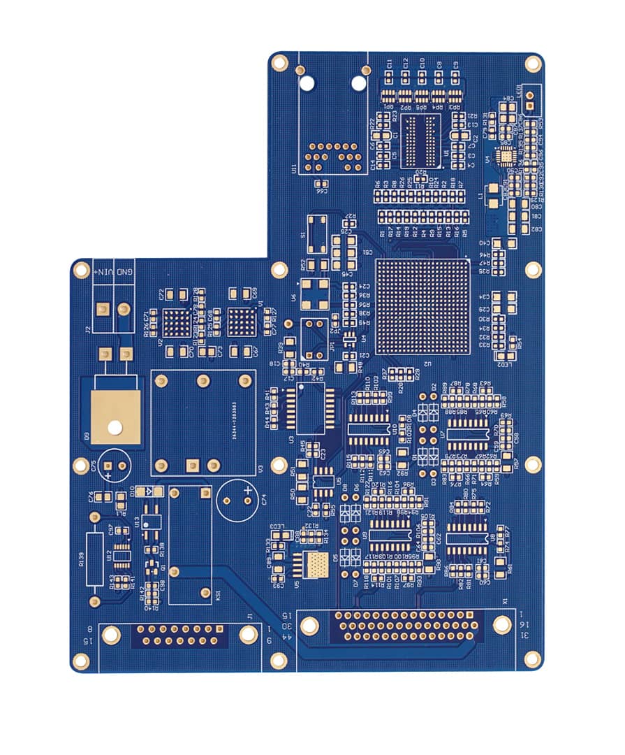
A Printed Circuit Board (PCB) serves as the physical backbone of electronics. It is a flat board made of non-conductive material (typically fiberglass-reinforced epoxy resin known as FR4) with thin copper traces etched onto its surface. These copper pathways serve as the "highways" that conduct electrical signals between electronic components. A PCB is essentially an empty canvas—it provides the structure and electrical connections but cannot perform any electronic function on its own.
Key PCB Insights:
Function: Provides mechanical support and electrical pathways.
Common Uses: Foundational platform for IoT devices, automotive systems, and consumer electronics.
The invention of PCBs significantly improved the efficiency of electronic production and the reliability of circuits. It enables compact designs with higher functionality and reduces the errors and unreliability associated with manual wiring.
1.1 Key components of a PCB
Substrate: The base material (usually FR4) that provides mechanical support
Copper Layers: Thin sheets of copper that form the conductive pathways
Solder Mask: A protective coating (often green) that insulates copper traces and prevents short circuits
Silkscreen: The top layer with text and symbols that label component positions for assembly
PCBA (Printed Circuit Board Assembly) refers to the process of mounting electronic components onto a PCB, transforming it from a passive structure into an active, functional circuit. Once assembled, the PCBA becomes the "brain" of an electronic device, capable of performing specific tasks like processing data, managing power, or enabling communication. Unlike a PCB, which is merely a bare board, a PCBA is a complete unit that has undergone assembly, soldering, and testing. The quality of PCBA dictates device reliability, influencing performance in aerospace, medical, or industrial systems.
PCB (Printed Circuit Board): The foundation base board itself.
Electronic Components: Resistors, capacitors, integrated circuits (ICs), diodes, transistors, connectors and other components that are mounted automatically or manually onto the PCBs.
Solder: The material that creates permanent electrical and mechanical bonds between components and PCB pads
Adhesives: Sometimes used to secure larger components against vibration
Traditional method where component leads are inserted through drilled holes
Provides stronger mechanical connections
Used for larger components and high-reliability applications like industrial machinery
2.2.3 Mixed Technology:
Combines SMT and THT for complex assemblies requiring both miniaturization and durability
3. PCB vs PCBA: Critical Differences
PCB is the foundational "bare board" etched with circuitry but devoid of components, whereas PCBA (Printed Circuit Board Assembly) is the complete, functional unit with all electronic components soldered and integrated.
PCB: A precision-engineered bare board consisting of laminated dielectric layers and etched copper circuitry that serves as the physical and electrical foundation.
PCBA: The finalized assembly where active and passive components are bonded to the PCB via SMT or DIP processes, transforming a static board into a functional electronic engine.
To better understand the differences between bare PCB and assembled PCB boards, the following table outlines their key aspects. It highlights the distinct characteristics in terms of their definition, functionality, manufacturing process, complexity, design, testing requirements, cost, and lead time.
3.1 Comparison Between PCB and PCBA
Aspect
PCB (Bare Board / Printed Circuit Board)
PCBA (PCBAssembled Board)
Definition
Raw board with copper traces, pads, and no components.
PCB with mounted electronic components
Functionality
Inert; enables connections but performs no action.
Active circuit capable of performing electronic functions
Higher (includes components, assembly labor and testing)
Lead Time
Faster turnarounds
2-4 weeks cycles
Applications
None on its own; serves as base for assembly
Powers all electronic devices from smartphones to medical equipment
4. Manufacturing Processes
4.1 PCB Manufacturing Processes
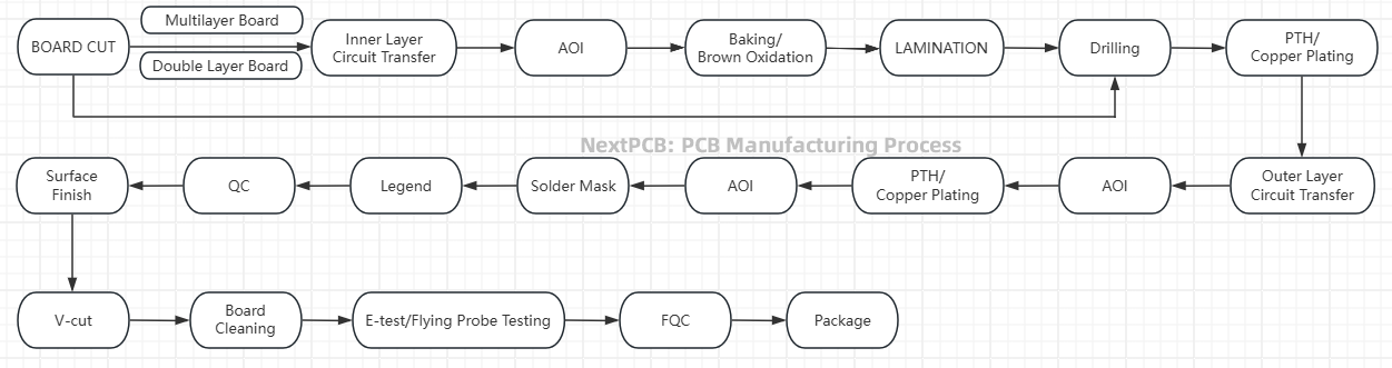
The journey from design to finished PCB involves several precise steps:
PCB Manufacturing Process - Flowchart
The PCB manufacturing process demands strict requirements, involving multiple complex steps to ensure the final product's quality, performance, and reliability. Multilayer boards offer higher integration and more complex circuit designs. Below is the PCB manufacturing process for multilayer PCBs, covering all stages from raw materials to finished products.
Step 1: Design & Gerber File Generation: Engineers create the circuit layout using CAD software, which is then converted into Gerber files (the industry standard for PCB manufacturing)
Step 2: Substrate Preparation: The base material (usually FR4) is cut to size and cleaned
Step 3: Copper Cladding: Thin copper foil is laminated onto the substrate
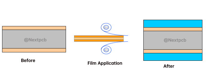
Step 4: Photoresist Application: A light-sensitive material is applied to the copper surface
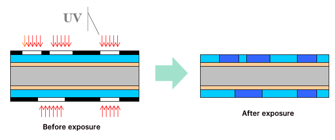
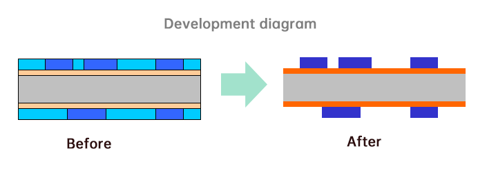
Step 5: Exposure & Development: The circuit pattern is transferred onto the photoresist using UV light, then unexposed areas are washed away
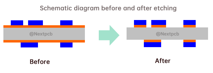
Step 6: Etching: Chemicals remove unwanted copper, leaving only the desired circuit pattern
Step 7: Drilling: Precision holes are drilled for component leads and vias (connections between layers)
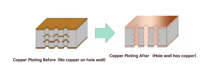
Step 8: Plating: Copper is plated inside holes to create electrical connections between layers
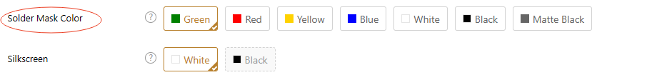
Step 9: Solder Mask Application: A protective coating is applied, leaving only pads exposed;
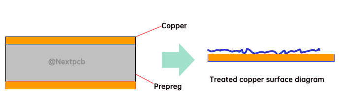
Solder mask is usually green, but there are other colors to choose from, and the functions are the same, the following are the solder mask color options listed in the PCB online quote options supported by Nextpcb:
Step 10: Silkscreen Printing: Component labels and symbols are printed onto the board
Step 12: Electrical Testing & Quality Control: Each board undergoes strict testing procedures to ensure conductivity and quality
The produced PCBs undergo electrical testing to ensure that all circuits are connected properly and meet design specifications.
4.2 PCB Assembly Processes
4.2.1 Files Required for PCB Assembly Manufacturing
4.2.1.1 BOM (Bill of Materials)
The BOM is a detailed list of all the components used in PCB assembly. It not only lists the part numbers, specifications, and quantities of each component but also includes unique identifiers, supplier information, and other relevant details.
If you plan to calculate prices online, each distributor may have different BOM format requirements. Therefore, when selecting a suitable and reliable supplier, it is important to ensure that the BOM file format is compatible with their online pricing system.
Gerber files are a standard file format used to describe all the design information for a PCB, including layer structure, copper patterns, pads, hole locations, and more. These files serve as the foundational documents for PCB manufacturing and assembly.
Centroid files are typically used in automated placement processes. They provide detailed information on the precise locations, rotation angles, and pickup points for each component on the PCB.
Once these documents are provided, NextPCB will conduct a thorough review based on the materials submitted. This includes evaluations such as DFA (Design for Assembly) audits to ensure that the design is optimized for efficient assembly and meets manufacturability standards.
HQDFM: Free PCB Design Analysis Tool with over 50 DFM and DFA Checks
4.2.2 PCBA Processes
Once the bare PCB is manufactured, the assembly process begins:
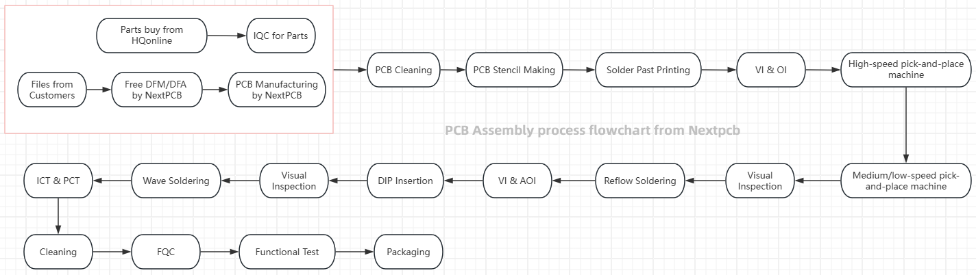
PCB Assembly Process - Flowchart
Step 1: Component Procurement & Inspection: Components are sourced and inspected for quality
Step 2: Solder Paste Application: Solder paste is applied to component pads using a stencil
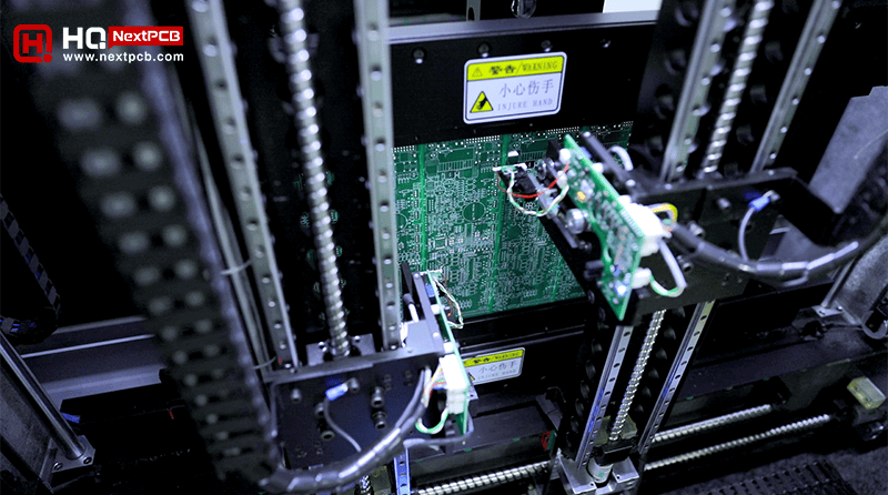
Step 3: Pick-and-Place: Automated machines place surface-mount components onto the PCB with high precision
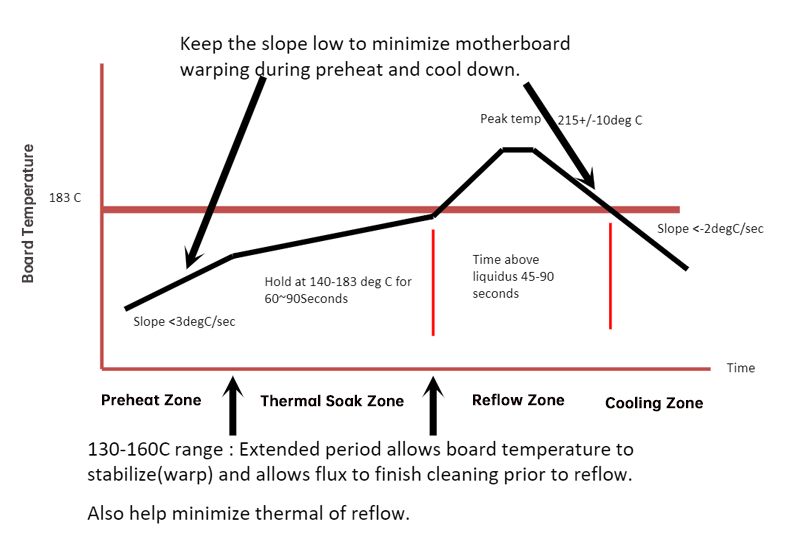
Step 4: Reflow Soldering: The PCB passes through a reflow oven, melting the solder paste to form permanent connections
Step 5: Through-Hole Component Insertion: THT components are inserted either manually or by automated machines
Step 6: Wave Soldering: For THT components, the PCB passes over a wave of molten solder to create connections
Learn more about How does Wave Soldering Mastery work in PCBA by:
Step 7: Inspection: Automated Optical Inspection (AOI) and X-ray inspection check for soldering defects
Step 8: Testing: Functional testing ensures the PCBA operates as designed
Step 9: Rework & Repair: Any defects found during inspection are corrected
Step 10: Cleaning: Flux residues are removed to prevent corrosion
Step 11: Final Quality Control: Comprehensive testing before shipment
The PCB assembly process is intricate and meticulous, with each step being crucial to ensuring high product quality and reliability. Through comprehensive inspections and potential rework, we strive to deliver dependable PCBA products to our customers.
Services such as DFM, DFA, and functional testing offered by NextPCB further reinforce our commitment to quality. By implementing effective process management and stringent quality control, we can enhance production efficiency, reduce defect rates, and meet market demands, all while prioritizing quality first.
5. Choosing PCB vs PCBA Services
Deciding whether you need a bare PCB or a fully assembled PCBA depends on your project stage and requirements:
5.1 Choose Bare PCB If
You're in the prototyping phase and need to test circuit designs
You have your own assembly capabilities
You need to source components separately for cost savings
You're building a custom solution with specialized components
5.2 Choose PCBA If
You need a turnkey solution ready for integration into your product
You lack assembly equipment or expertise
Your design requires specialized assembly techniques (fine-pitch SMT, BGA)
You want to reduce supply chain complexity by working with a single vendor
Tip for Engineers: Compare suppliers on IPC compliance (IPC-A-610), testing protocols, and turnkey capabilities (procurement to shipping).
6. Choosing a Reliable PCB/PCBA Manufacturer
Selecting the right manufacturing partner is critical to project success. Look for these key qualities:
Industry Experience: Look for manufacturers with experience in your specific industry
Certifications: ISO 9001, IPC-A-610 (electronics assembly standard), and relevant industry certifications
Technical Capabilities: Advanced equipment for complex designs and tight tolerances
Quality Control Processes: Comprehensive testing and inspection protocols
Turnaround Time: Flexible lead times to meet your project schedule
Customer Support: Responsive engineering support throughout the process
7. FAQs
What is the difference between PCB and PCBA?
A PCB is a bare board with copper traces, while a PCBA is a PCB that has undergone the assembly process with electronic components mounted, making it functional.
Which is more expensive: PCB or PCBA?
PCBA is typically more expensive than a bare PCB because it includes the cost of components, assembly labor, and testing.
How long does it take to manufacture a PCB vs PCBA?
PCB manufacturing usually takes 1-3 weeks, while PCBA assembly adds another 1-2 weeks depending on component availability and complexity.
Can a PCB be reused after assembly?
While technically possible, reusing a PCB is generally not practical due to soldering residue, component removal damage, and potential copper trace damage.
What are the most common PCB surface finishes?
Common finishes include HASL (Hot Air Solder Leveling), ENIG (Electroless Nickel Immersion Gold), OSP (Organic Solderability Preservative), and immersion silver or tin.
How do I ensure my PCB design is manufacturable?
Work with your manufacturer early in the design process for DFM (Design for Manufacturability) feedback, and use standard design rules for trace widths, spacing, and component placement.
8. Conclusion
Understanding the distinction between PCB and PCBA is essential for anyone involved in electronics design, manufacturing, or procurement. While the PCB forms the critical foundation with its conductive pathways, it's the PCBA assembly process that breathes life into the circuit, enabling the electronic devices that power our modern world.
Whether you need a simple single-layer PCB for a hobby project or a complex multi-layer PCBA for industrial equipment, partnering with an experienced manufacturer is key to achieving reliable, high-quality results. By considering your specific application requirements, budget constraints, and production timeline, you can make informed decisions about whether to source bare PCBs, assembled PCBAs, or turnkey solutions.
At NextPCB, we specialize in both PCB manufacturing and turnkey pcba service, offering end-to-end solutions from low-volume prototyping to mass production. Our state-of-the-art facilities and rigorous quality control ensure your electronic assemblies meet the highest standards of performance and reliability.
In project development, time is critical – and NextPCB delivers. We're your one-stop solution for PCB manufacturing and assembly, turning your designs into reality with speed and precision. From high-quality bare boards to advanced PCB Assembly, NextPCB handles both prototypes and mass production. Our expert DFM support ensures top-tier quality and efficiency. Partner with us to streamline your supply chain and accelerate your projects with reliable, trusted PCB solutions. Last updated 2025/9/18.


 NextPCB Capabilities
 PCB Assembly
 Layer Buildup
 SMD-Stencils
 PCB Design-Aid & Layout
 Mechanics
 Surface
 Quality
 Drills & Throughplating
 Factory & Certificate