

 NextPCB Capabilities
 PCB Assembly
 Layer Buildup
 SMD-Stencils
 PCB Design-Aid & Layout
 Mechanics
 Surface
 Quality
 Drills & Throughplating
 Factory & Certificate


Introduction
This guide provides a comprehensive yet practical checklist for DFM and DFA, designed specifically for engineers and PCB professionals. It cuts through the jargon to focus on actionable steps and key considerations that directly impact project efficiency, cost, and product quality. By presenting a framework for proactive design reviews and demonstrating the capabilities of automated tools like HQDFM, this article aims to help you streamline your workflow and avoid common manufacturing pitfalls before they cause delays.
Part 1: The Strategic Value of DFM: The Key to Efficiency, Cost, and Reliability
1.1 DFM: A Practical Path to Efficient Development
DFM, or Design for Manufacturability, is simply about ensuring your design can be produced smoothly and successfully on the first try after it's handed over to the factory. It's not a complex theory; rather, it's the practice of integrating manufacturing and assembly expertise into the design stage from the very beginning. The core goal is straightforward: to avoid rework, save time, and reduce costs.
Traditionally, designers focus solely on function, while manufacturers prioritize yield. This can lead to a conflict where the factory modifies a design for production ease, but these changes may contradict the designer's original electrical performance intent, ultimately causing frustration and delays. DFM puts you in control from the start, ensuring your design vision and manufacturing capabilities are perfectly aligned, so you're not left at the mercy of factory modifications.
1.2 Automation: An Inevitable Choice for Complex Designs
Modern PCBs often contain thousands of components and connections, and trying to find every potential issue with the naked eye is simply impractical. A design file might look perfect, but once it gets to the factory, a host of small problems can surface. This endless cycle of rework and inspection is not only time-consuming but also incredibly inefficient. The traditional linear workflow of "design-process-manufacture" suffers from poor information flow. Worse, if you wait until the design is finalized to perform a DFM review, any small change can have a domino effect, with modification costs increasing exponentially. Therefore, moving DFM to the front of the process and using automated tools is a necessary step to handle the complexity of modern hardware design. Automated DFM tools can proactively identify and resolve potential performance and reliability issues before the design files are even submitted, reducing manufacturing risks by up to 90%.
1.3 The Ultimate Value of DFM: Cost, Cycle Time, and Quality
The value of DFM can be condensed into three core pillars: minimizing cost, shortening the development cycle, and maximizing quality. Together, they form the "Golden Triangle" of modern product development.
- Cost Control: DFM's primary mission is to save money. Through DFM analysis, you can proactively identify and optimize design features that require special processes or tools, such as ultra-thin walls or narrow areas. Modifying these high-cost features in the design stage is far cheaper than doing it during manufacturing. Additionally, collaborating with the procurement team early in the schematic phase and using components from an Approved Vendor List (AVL) can prevent production halts and extra costs from using obsolete (EOL) or hard-to-find components with long lead times.
- Project Acceleration: Proactively performing DFM helps you avoid repetitive design changes and significantly shortens the product development cycle. A comprehensive DFM-reviewed design file allows the factory to provide an instant quote and begin production immediately, without the need for endless communication and modifications from the CAM team, saving a huge amount of time.
- Quality Assurance: DFM can also help you fix unseen, long-term hidden dangers. For example, thermal management design for high-power components. If heat cannot dissipate properly, components can overheat, leading to performance degradation or even failure. This directly impacts the product's lifespan and reliability. A professional DFM checklist must include these considerations, as they are crucial for a product's long-term stability.
The table below provides a clear comparison of the significant differences between traditional and modern DFM processes.
Table 1: Traditional vs. Modern DFM Processes
|
Feature |
Traditional DFM Process |
Modern DFM Process (Designer-Led) |
|
DFM Performer |
Manufacturer (Reactive) |
Designer/Engineer (Proactive) |
|
DFM Timing |
After design is finalized, or even before tooling |
Early stage of product design |
|
Main Goal |
Ensure manufacturing yield, avoid production stops |
Optimize design, improve product performance, reliability, and cost-effectiveness |
|
Problem Discovery |
During manufacturing |
During design |
|
Design Modification Cost |
High, increases exponentially (may involve changes to multiple components) |
Lowest, only requires adjustments within the design software |
| Impact on Project Cycle |
Rework leads to extended project timelines |
Avoids rework, significantly shortens the development cycle |
|
Impact on Product Quality |
Manufacturer's reactive changes to improve yield may sacrifice electrical performance |
Proactive design optimization ensures consistency between manufacturing and electrical performance |
Part 2: Essential DFM Checklist: Practical Points and Key Considerations
This checklist is not just a simple list of design rules; it uncovers the most fundamental issues behind DFM from multiple dimensions, including manufacturing, assembly, testing, and supply chain. An engineer's DFM capability is not about isolated parameters, but about understanding their interactions and their far-reaching impact on the product's entire lifecycle.
2.1 Core Manufacturing Process Checks: Ensuring Production Feasibility and Product Quality
Manufacturability is the foundation of DFM, ensuring the design can be effectively transformed into a physical product.
- Copper and Via Design: Copper clearance and trace width must meet both electrical performance requirements and the manufacturer's capabilities. Annular ring width is also crucial, ensuring proper drill alignment tolerance to prevent broken rings. Via-in-pad is a complex DFM issue, as the risk lies in solder paste flowing into the via during reflow soldering, leading to cold or bad solder joints. A professional DFM review will assess the via-in-pad risk based on the manufacturer's capability and may suggest plugging the vias to mitigate the risk.
- Component Placement and Assembly: Component layout is central to Design for Assembly (DFA). Inadequate spacing between pads and components is a common pitfall, increasing the risk of tombstoning or bridging, which reduces assembly efficiency and yield. For BGA or high-density component areas, sufficient space must be left to ensure smooth SMT. Additionally, silkscreen should not overlap with pads, as it can affect the effective soldering area.
- Mechanical Dimensions and Materials: The mechanical design of the PCB also requires DFM consideration. The choice of board thickness, slots, and shaping tolerances directly relates to the product's mechanical strength and manufacturing cost. Opting for non-standard materials or stack-ups that require special processes can significantly increase material procurement lead times and costs, potentially pushing the design to the limits of manufacturing and delaying the overall project.
2.2 Reliability and Testability Considerations: Extending Product Lifespan
A successful product must not only be manufacturable but also operate reliably in the field.
- Design for Testability (DFT): A lack of DFT can lead to high production line failure rates, long debugging cycles, and difficulty in quickly pinpointing the root cause. This directly translates to higher production control costs. Therefore, a DFM checklist must include DFT checks: adding test points for key signals, ensuring probe accessibility, and, if possible, performing 3D simulations to check for interference.
- Thermal Management Design: DFM's scope is expanding beyond basic geometric constraints to include professional fields related to performance and reliability. High-power components in modern products continuously generate heat during operation. If thermal management is inadequate, heat accumulation can lead to component overheating, causing performance degradation, a shortened lifespan, or even thermal runaway and safety incidents. Therefore, DFM should consider thermal layout in the design phase, such as using large copper areas or thermal vias, deeply integrating DFM with DTM (Design for Thermal Management).
> Recommend reading: Fundamentals of PCB Thermal Design | NextPCB
2.3 Supply Chain and Project Management: Ensuring Project Delivery
The DFM perspective must extend beyond the design itself to encompass the entire project and supply chain.
- Component Lifecycle Management: A seemingly simple component choice can hide huge supply chain risks. Using obsolete (EOL) or difficult-to-procure (NRND) components can lead to production stalls, increased procurement risk, and inconsistent batch quality. Engineers should work with the procurement team or EMS factory in the schematic phase and use tools like Octopart and SiliconExpert to verify component lifecycle status, eliminating risks from the source.
- Impact of Lead Time: DFM is not just about manufacturability; it's also about project delivery time. Pushing a design to the manufacturing limit, such as choosing a stack-up, via type, or surface finish that requires special materials or processes, can slow down every stage. Therefore, when finalizing a design, engineers must proactively ask the contract manufacturer or EMS provider: "How long will this take to manufacture?"
> Recommend reading: DFM, DFMA, DFA. Part 1. Kicad and Online Gerber Viewer
The table below summarizes the core DFM checklist items and common pitfalls.
Table 2: Core DFM Checklist and Common Pitfalls
|
DFM Check Item |
Common Pitfall |
Impact on Cost/Quality/Timeline |
Engineer's Solution |
|
Copper Spacing |
Too small, doesn't meet manufacturer's capability |
Manufacturing failure, or requires extra processing cost |
Set a safety margin in design rules and sync with manufacturer's specifications |
|
Pad Spacing |
Too small, insufficient space between components |
Easily leads to bridging, tombstoning, high assembly failure rate, requires manual rework |
Check IPC-7351 standards and SMT factory requirements, leave enough space |
|
Via-in-Pad |
Via in pad is not plugged |
Solder paste flows in, causing cold or bad solder joints, affecting reliability |
Determine manufacturer's plugging capability and explicitly request plugging in the DFM report |
|
Testability (DFT) |
No test points for key signals |
High production line failure rate, long debugging cycle, difficult to locate issues |
Reserve test points in the design phase and ensure probe accessibility |
|
Component Lifecycle |
Using EOL or long lead time components |
Production stalls, requires urgent design changes, increases procurement cost |
Collaborate with the procurement team early in design, use components from the AVL |
|
Special Processes |
Choosing non-standard stack-ups, via types, or surface finishes |
Extends material procurement cycle, increases manufacturing cost and project delay risk |
Communicate with the factory before finalizing the design to understand manufacturing lead times |
Part 3: HQDFM in Action: Turning Theory into Productivity
3.1 The Rise of Automated DFM: Why Manual Review is Obsolete
Faced with increasingly complex PCB designs, automated DFM tools are a necessary choice to solve the problem of "invisible" issues that human eyes can't catch. Tools like NextPCB's HQDFM can automatically check over 20 DFM issues in a second, and its desktop suite provides over 1,200 DFM and DFA (Design for Assembly) checks.
The core value proposition of automated DFM tools lies not just in their speed but in their "depth" and "synergy." Automated DFM tools use machine learning algorithms and deep analysis to proactively identify and resolve potential performance or reliability issues before the design files are submitted, reducing manufacturing risks by up to 90%. What's more, HQDFM is developed and maintained by NextPCB's practicing engineers, ensuring its analysis rules are highly synchronized with real-world manufacturing capabilities, achieving a truly "zero-gap" DFM.
> HQ NextPCB Introduces New PCB Gerber Viewer: HQDFM Online Lite Edition
3.2 HQDFM Functional Analysis and Application
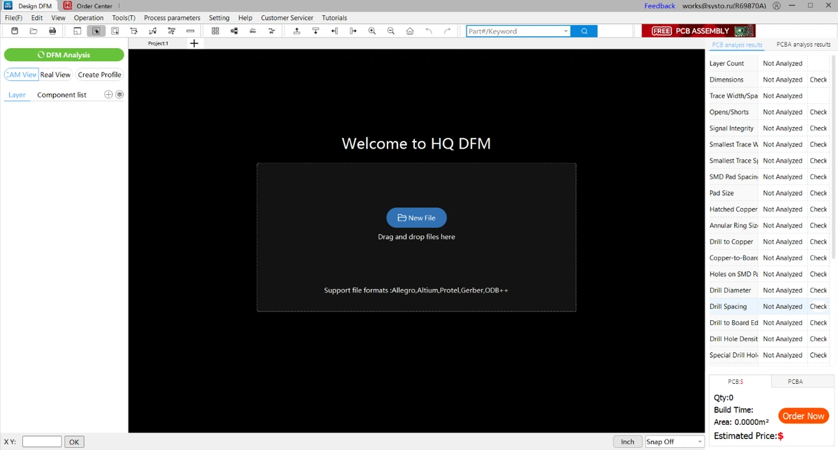
HQDFM is a professional DFM tool designed to simplify the designer's workflow and provide in-depth analysis.
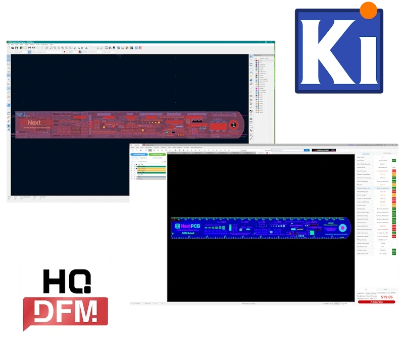
- Smart File Recognition and Multi-Format Support: HQDFM is more than just a Gerber viewer; it also supports ODB++ and native KiCad files (.kicad_pcb), and can automatically identify and align each layer. This smart import feature greatly simplifies the designer's workflow and reduces errors caused by file format issues.
- Multi-Dimensional Analysis and One-Click Reports: HQDFM automatically checks for issues like copper-to-edge clearance, electrical nets, and solderability, and generates detailed DFM reports with actionable improvement suggestions. Additionally, it provides various measurement tools to measure the straight-line distance between any two points, two object edges, or between nets, which is crucial for confirming design clearances and signal integrity.
- Core Feature Demonstration:
- - Smart Panelization and Route Length Calculation: HQDFM offers a smart panelization tool that allows you to customize the process edge, spacing, and number of boards, and calculates the total route length for the final PCB and the board material utilization rate, helping designers optimize costs in the design phase.
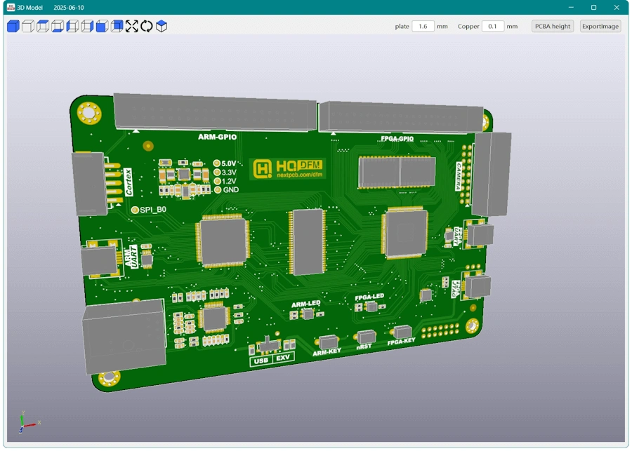
- - 3D Simulation Preview: The tool provides a realistic 3D simulation, giving designers a "what you see is what you get" view to proactively discover potential assembly or structural issues.
3.3 Case Study: How HQDFM Addresses the "Via-in-Pad" Risk
Using the complex DFM issue of via-in-pad as an example, we can clearly see the practical value of HQDFM. While via-in-pad designs save space, they also pose a significant manufacturing risk because solder paste can flow into the via, leading to cold or bad solder joints.
In a traditional workflow, this issue would typically be discovered by the manufacturer during their DFM review, leading to a request for design modification, which can cause rework, project delays, and extra costs.
HQDFM's solution:
- 1. Automatic Identification: HQDFM automatically scans the PCB file and precisely identifies all via-in-pad locations.
- 2. Risk Alert: The tool's internal rule library (based on industry-wide manufacturing capabilities) determines whether these via-in-pads pose a manufacturing risk and provides a clear warning.
- 3. Optimization Suggestions: In the detailed DFM report, HQDFM suggests whether the vias need to be plugged or if the pad design should be adjusted to avoid issues.
- 4. Seamless Integration: Once the design is corrected, the designer can seamlessly transfer the files and data with one click to NextPCB for quoting and manufacturing, with no need for data re-entry.
> Recommend reading: How to avoid shorts and opens in PCB Design using Design for Manufacture (DFM) tools?
3.4 Extended Capability: HQDFM's DFA Analysis
DFM focuses on the manufacturability of the bare board, while DFA (Design for Assembly) goes a step further by ensuring efficient and error-free component placement and soldering for automated machinery. A design that has undergone DFA analysis can effectively prevent production bottlenecks, reduce manufacturing costs, and optimize for high-volume production.
The HQDFM desktop suite provides over 1,200 DFM and DFA checks, and its core DFA capabilities include:
- Component Layout and Spacing: HQDFM automatically checks the spacing between component pads and the component body, ensuring pick-and-place machines have enough room to operate. This helps avoid issues like bridging and tombstoning caused by insufficient spacing, which is particularly important for BGAs and high-density areas, and can significantly improve assembly yield.
- Pad Design and Surface Finish: For fine-pitch components (e.g., QFPs with a pitch less than 0.5mm) or small BGAs (pad diameter less than 0.25mm), pad flatness is crucial. HQDFM will recommend using a flatter surface finish like ENIG (Electroless Nickel Immersion Gold) instead of HASL (Hot Air Solder Leveling) to ensure soldering quality and reliability. >HASL vs ENIG: An Ultimate Guide on Surface Finish
- Through-Hole Size Check: For through-hole components that require wave soldering, the hole size must be appropriate to ensure solder can flow through smoothly. HQDFM can verify if the through-hole dimensions are appropriate for the component leads to prevent poor soldering.
NextPCB DFM Tool Exclusive Offer: Get a $10 Coupon Every Month!
The table below links the theoretical DFM checklist items with the specific functions of HQDFM, showing how an automated tool can turn abstract DFM concepts into actionable, quantifiable operations.
Table 3: Core DFM Checklist and Corresponding HQDFM Functions
|
DFM Check Item (Theory) |
Common Pitfall |
HQDFM Function (Practice) |
|
Manufacturing Tolerance Check |
Copper spacing/trace width/annular ring is too small |
Automated DFM report check, electrical net measurement tools |
|
Testability Check |
No test points, probes are inaccessible |
Automated DFM report check, 3D simulation preview |
|
Assembly Check |
Insufficient component spacing, silkscreen on pads |
Automated DFM report check, 3D simulation preview |
|
Cost Optimization |
Non-standard panelization, low board material utilization |
Smart panelization and route length calculation, board material utilization rate calculation |
Part 4: The Future of DFM: Data-Driven and Collaborative Evolution
4.1 Big Data and AI-Driven DFM: Pushing the Boundaries
Automated DFM tools are not stopping at rule-based checks. They are beginning to use machine learning algorithms to process massive amounts of CAD file data, such as holes, volume, and wall thickness. Future DFM tools will evolve from passive checking tools into proactive "design consultants," capable of predicting manufacturing yield based on big data analysis and even intelligently generating optimized design solutions based on goals like cost, lead time, and yield.
4.2 Seamless Collaboration Between Design and Manufacturing: Towards True Integration
The ultimate form of DFM is seamless collaboration among design, manufacturing, supply chain, and test teams. In the traditional model, information silos lead to repetitive work, misunderstandings, and unnecessary rework, ultimately causing project delays and increased costs. DFM tools will become the bridge connecting these isolated parts. By providing a shared data platform where all stakeholders can review and contribute to the design in its early stages, true "collaborative engineering" can be achieved, maximizing the value of DFM.
Conclusion
DFM is no longer an optional step; it is an essential strategic capability in modern hardware development. It represents a fundamental shift from the traditional "design-manufacture" linear model to a parallel "smart manufacturing-collaboration" model. A skilled engineer is not only proficient in every technical DFM checkpoint but also deeply understands the underlying business logic and strategic value.
By moving DFM to the front of the process and leveraging automated tools like HQDFM at NextPCB, designers can solve manufacturing, assembly, testing, and supply chain issues at the source. This ensures a seamless transition from concept to mass production, achieving the golden triangle of cost, cycle time, and quality, and giving businesses a head start in fierce market competition. DFM is the strategic foundation for product success and the inevitable path for hardware development to enter the era of smart manufacturing.


