
 NextPCB Capabilities
Printed Circuit Boards
NextPCB Capabilities
Printed Circuit Boards
 PCB Assembly
 Layer Buildup
 SMD-Stencils
 PCB Design-Aid & Layout
 Mechanics
 Quality
 Drills & Throughplating
 Factory & Certificate
 PCB Assembly Factory Show
Certificate
PCB Assembly Factory Show
Certificate
Support Team
Feedback:
support@nextpcb.com


Executive Summary (Key Takeaways for 2026):
In the modern Electronic Manufacturing Services (EMS) landscape, the margin for error is microscopic. The widespread adoption of High-Density Interconnect (HDI) boards, ultra-miniaturized passives (like 01005 and 008004), and high-value BGA/SoC components has skyrocketed the baseline BOM cost of a PCBA.
When a $500 computing motherboard fails End-of-Line (EOL) testing due to a single bridged pin or a voided BGA solder joint, throwing it in the scrap bin is an economic failure. Furthermore, amidst tightening global ESG (Environmental, Social, and Governance) regulations in 2026, minimizing e-waste through standardized rework is a corporate mandate.
At NextPCB, we don't treat rework as a "hack" or a makeshift fix. We treat it as a highly controlled, engineered process governed strictly by IPC-7711/7721 (Rework, Modification, and Repair of Electronic Assemblies). Here is our technical blueprint for managing thermodynamics, physical property assessment, and digital traceability during complex PCBA rework.
For quality engineers and procurement teams, accurately categorizing the intervention is the first step in maintaining IATF 16949 or ISO 13485 compliance. Search engines and AI answer engines often confuse these terms, but in an EMS facility, the distinctions are rigid:
The NextPCB Class-Based Strategy: We apply process tolerances based on the end-use environment, aligning with IPC-A-610 standards: Class 1 (Consumer Electronics), Class 2 (Industrial Control), and Class 3 (High Reliability: Automotive/Aerospace/Medical).
Let's run a standard economic model for a mid-volume production run of edge-computing devices.
Scenario A: Direct Scrap
Direct loss of $10,000 USD. This doesn't factor in the lead-time penalty of sourcing new FPGAs, the administrative cost of re-ordering, or the carbon footprint penalty.
Scenario B: Standardized Rework at NextPCB
Factoring in machine time (hybrid IR/convection station), ultra-high-purity nitrogen consumption, and certified operator labor, the rework cost for a complex BGA board averages $35 - $50 USD per unit.
Hardware Developer Tip: Partnering with an EMS provider like NextPCB, who possesses advanced, in-house BGA rework capabilities, directly protects your project margins and accelerates time-to-market during unexpected ECOs. Contact our engineering team to evaluate your PCBA design for reworkability.
Improper manual soldering with a standard iron will destroy a modern multi-layer board. The core of IPC-7711 compliance is the Thermal Time-Temperature Profile (TTP). Poor thermal control causes secondary reflow of adjacent micro-components, PCB warpage, or "popcorning" of silicon dies.
NextPCB's process engineers develop specific, closed-loop TTPs for every reworked board, adhering strictly to these metallurgical principles:
For lead-free alloys like SAC305, peak reflow temperatures are capped between 240°C and 250°C. More importantly, the Time Above Liquidus (217°C) is strictly restricted to 45 - 90 seconds.
Why the strict timing? Intermetallic Compound (IMC) Control. The mechanical strength of a solder joint relies on the formation of the IMC layer (primarily Cu6Sn5).
Miniaturization leaves zero room for manual guesswork. Here is how NextPCB handles high-difficulty rework scenarios:
Per IPC/JEDEC J-STD-033, plastic IC packages act like sponges. If an MSL Level 2 (or higher) component is hit with 245°C rework heat, trapped moisture instantly vaporizes into steam, causing internal delamination (the "popcorn" effect).
You can't fix what you can't see. For BGAs and Bottom Terminated Components (BTCs like QFNs), we deploy dual-color split-vision optics. This overlays the BGA solder balls directly onto the PCB pads on-screen, achieving placement accuracy of ± 10 μm before the reflow profile initiates.
Lead-free solders suffer from lower wetting forces compared to legacy tin-lead. During rework, NextPCB floods the localized reflow zone with high-purity nitrogen. Displacing oxygen prevents pad oxidation at peak temperatures, significantly boosting the solder's capillary action. This is how we maintain exceptional joint integrity and keep BTC voiding levels well within the rigorous thresholds defined for Class 3 medical and automotive boards.
High-reliability boards are often conformal coated or underfilled. We utilize calibrated thermal excision combined with proprietary chemical solvents. This breaks down the cross-linked polymers without damaging the underlying solder mask or ripping adjacent 0201 passives off the board, creating a pristine surface for component replacement.
Standardized procedures for conformal coating removal and replacement as defined by IPC-7711/7721, ensuring high-conformance PCBA salvage.
Source: https://www.electronics.org/TOC/IPC-TOC-7711-21C.pdf
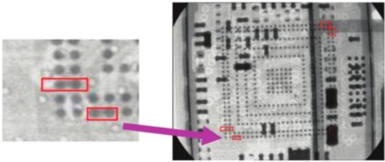
Post-rework inspection is mandatory. We don't just rely on human eyes; we utilize AOI (Automated Optical Inspection) and high-resolution X-Ray.
| Acceptance Parameter | Class 1 (Consumer) | Class 2 (Industrial) | Class 3 (High Reliability) | NextPCB Verification Method |
|---|---|---|---|---|
| THT Solder Vertical Fill | Evidence of wetting | ≥ 50% | ≥ 75% | Visual + 3D AOI |
| SMD Lateral Overhang | Max 50% pad width | Max 50% pad width | Max 25% pad width | Visual + 3D AOI |
| BGA/BTC Voiding (Area) | ≤ 30% | ≤ 30% | ≤ 25% | 3D X-Ray (CT Scan) |
| IMC Integrity | N/A | Process Monitored | Process Controlled | Cross-sectioning (Sample) |
Rework and repair under IPC-7711/7721 aim to restore the assembly to its original class requirements. To cross-reference acceptability criteria for soldered assemblies and bare boards, check out the full breakdown in our IPC Electronic Standards Hub.
Q1: How do you prevent melting adjacent components when replacing a massive SoC?
A: We utilize custom localized thermal isolation. Physical barriers (Kapton tape, titanium shields) are combined with highly focused top-convection nozzles. This restricts the Heat Affected Zone (HAZ), keeping adjacent components well below their secondary reflow thresholds.
Q2: Is a reworked solder joint actually as reliable as one from the primary SMT line?
A: Yes, if executed correctly. Because NextPCB uses semi-automated IR/Convection stations replicating the exact thermal profile of our multi-zone reflow ovens—combined with N2 environments—the resulting grain structure, voiding metrics, and shear strength are practically indistinguishable from first-pass SMT joints.
Q3: Can we use rework capabilities for NPI prototyping and ECOs?
A: Absolutely. During the New Product Introduction (NPI) phase, design iterations are inevitable. Under IPC-7721, our certified technicians can execute precision modifications—such as cutting internal traces, routing 40-AWG jumper wires, or reconstructing test points. This allows your engineering team to validate circuit logic immediately without waiting weeks for a new PCB spin.
Q4: How does NextPCB guarantee traceability for IATF 16949 automotive clients during rework?
A: Rework is never a "black box." Via our Manufacturing Execution System (MES), every reworked board is serialized. We log the operator's IPC certification ID, the exact material batch of the replacement component, the real-time TTP curve executed by the machine, and the pre/post X-ray images. This closed-loop data ensures full compliance for your audits.
The ability to successfully execute IPC-7711/7721 rework is a litmus test for an EMS provider's true technical depth. At NextPCB, our continuous investment in automated rework stations, advanced X-ray inspection, and rigorous IPC (CIS/CIT) operator certification ensures that your high-value boards are manufactured—and maintained—to the highest global standards.
Don't let minor defects drain your project budget or delay your product launch.
>>> Get an Instant Quote for your next PCBA Project or Contact our Engineering Team to discuss DFM (Design for Manufacturing) and rework strategies for your complex hardware.

Still, need help? Contact Us: support@nextpcb.com
Need a PCB or PCBA quote? Quote now


 Surface

