What is 2-Layer PCB?
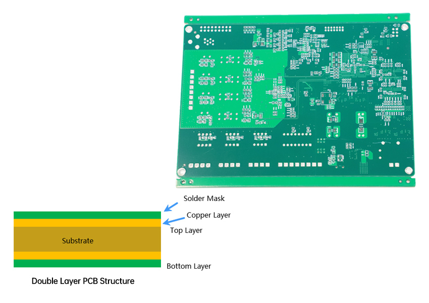
2-layer PCB is a printed circuit board with two conductive copper traces. These two layers are located on the top layer and bottom layer of the substrate, and are typically connected by plated through-holes, allowing current to transmit between the two layers. Compared to a Single layer PCB which has only one conductive copper layer, a Double layer PCB significantly increases wiring space and component density, making it possible to design more complex circuits.
A two-layer PCB is not simply two single-sided boards stacked together. It is made by laminating a dielectric substrate (such as Fr-4 material) with two copper foil layers under high temperature and pressure. This structure provides the physical foundation for mechanical support and electrical connections.
2-Layer PCB Structure and Material Analysis
Understanding the composition of a two-layer PCB is the starting point for design and manufacturing. Its core components include:
- Substrate: The skeleton of the two-layer PCB, typically made of Fr-4 material. Fr-4 is a composite material of epoxy resin and glass fiber cloth, providing good insulation, mechanical strength, and heat resistance, and is cost-effective. Of course, special applications may choose more advanced materials like PTFE, Rogger or Aluminum, but the cost will increase accordingly.
- Copper Layers: There is a layer of conductive copper foil on both the top and bottom sides of the substrate. These copper foils are etched to form the traces, pads, and functional areas of the circuit. The thickness of the copper foil is a key parameter, with common thicknesses including 0.5 oz, 1 oz, 2 oz, or even higher. The thicker the copper foil, the greater its current-carrying capacity, but the cost also increases.
- Solder Mask: A protective layer covering the copper traces, usually green, but also available in other colors like blue, red, black, purple. The main purpose of the solder mask is to prevent copper traces from oxidizing during soldering, prevent solder from shorting to areas that should not be connected, and provide electrical insulation.
- Silkscreen: The top-most marking layer, used to print component identifiers, reference numbers, logos, test point markings, and other non-conductive information. It is usually in white font but can also be in other colors.
- Vias: In a double layer PCB, vias are plated drilled holes that connect conductive traces on the top and bottom layers. They allow signals and power to flow vertically through the circuit board. For 2-layer PCBs, through-hole vias, which completely penetrate the board, are typically used.
- Pads: Conductive areas used to connect the pins of electronic components or surface mount components. Components can be soldered by inserting them into the drilled holes using through-hole technology (THT), or by directly soldering them onto surface pads using surface mount technology (SMT).
2-Layer PCB Manufacturing Process
The production process of a dougble sided PCB is a series of precise chemical and physical operations, mainly including the following steps:
- Material Cutting: Cutting large copper-clad laminates into standard sizes suitable for the production line.
- Drilling: Precisely drilling component holes and vias according to the design files (Gerber files).
- Chemical Copper Deposition & Plating: This is a key step to achieve layer-to-layer conductivity. Through the chemical copper deposition process, a thin layer of chemical copper is formed on the non-conductive hole walls, making them conductive. Subsequently, electroplating is performed to thicken the copper on the hole walls, ensuring reliable conductivity.
- Outer Layer Imaging: Through lamination of photosensitive dry film, exposure, and development, the circuit design pattern is accurately transferred onto the copper layers.
- Pattern Plating & Tin Plating: The developed circuit pattern is plated again to further increase the copper thickness. A layer of tin (or nickel-gold, etc.) is then plated on the copper traces that need to be preserved, acting as an etchant resist.
- Etching: A chemical solution is used to remove the excess copper foil not protected by the tin layer, forming the desired circuit trace pattern.
- Stripping: The dry film previously used to protect the copper traces is removed, exposing the final copper circuit pattern.
- Solder Mask: A layer of liquid or dry film solder mask ink is evenly coated on the entire circuit board surface, and through exposure and development, the solder mask is only retained on the non-pad areas.
- Silkscreen Printing: Component symbols, markings, etc., are printed on top of the solder mask using screen printing technology.
- Surface Finish: The exposed pads and vias are surface-treated to prevent oxidation and provide good solderability. Common surface finishes include HASL/Lead-Free HASL, ENIG, and OSP. Special surface finish is rarely used on double layer pcb, such as ENEPIG, Immersion Silver/Tin, Electroplated Gold, and Gold Finger Plating. These are generally used on multilayer PCBs or products in very special fields.
- CNC Machining: A CNC router or punching mold is used to cut the PCB from the larger panel according to the designed outer shape.
- Electrical Test: A 100% open/short circuit test is performed on each PCB to ensure that all circuit connections meet the design requirements.
- Final Inspection & Packaging: The PCB is inspected for physical defects, and then packaged for shipment.
How much does a 2-layer PCB cost?
2 layper PCB cost usually range from $0.1 to $5/5pcs for 24 hours quick-turn with Fr-4 material, size less than 100mm*100mm, 1.6mm board thiness, 1oz copper weight, and a HASL surface finish.
The cost of a two-layer PCB is influenced by a variety of factors. Understanding these factors helps in optimizing the design and controlling the project budget:
- Substrate Material: Fr-4 is the mainstream choice and is low-cost. However, if special performance materials (like high Tg, high-frequency boards) are chosen, the price will increase significantly.
- Board Thickness and Copper Weight: 1.6mm standard board thickness with 1oz Copper has a regular price. However, special thicknesses can affect the cost. Thicker copper foil leads to higher raw material costs, and also increases the difficulty of etching, raising process costs.
- Size & Panel Utilization: The size area of the PCB is the most direct cost factor. Without affecting electrical performance, optimizing the board size to improve the utilization of the production panel can effectively reduce the unit cost.
- Production Quantity & Lead Time: The cost of a PCB order is heavily influenced by its production quantity and required lead time. For small-batch prototyping, the unit price is significantly higher. This is because non-recurring costs—such as tooling, programming for drilling, and initial equipment setup—are fixed regardless of the order size. When these costs are spread across just a few boards, the per-unit price becomes very high. Additionally, prototyping often involves preparing extra materials to prevent scrap, which lowers overall material utilization. For larger orders, these fixed costs are distributed over more units, drastically lowering the per-board price. Finally, rush orders often incur an additional expediting fee to cover the cost of disrupting standard production schedules and reallocating resources.
However, Don't worry too much, to let users experience NextPCB's quality and service, NextPCB provides many discounts, double-sided PCB prototype as low as $0.1/10pc in 24 hours turnaround.
- Process Complexity:
- Trace Width/Spacing: Finer trace widths and smaller trace spacing (e.g., 4/4 mil or less) demand higher production precision and result in a lower yield, thereby increasing costs.
- Drilling Parameters: The number and size of holes. Too many holes or holes that are too small (e.g., micro-vias smaller than 0.1mm) will increase drilling time and difficulty, driving up costs.
- BGA and Special Packages: PCBs with high-density BGA packages require higher manufacturing precision, which can also increase costs.
- Surface Finish: The cost of different surface finish options varies greatly. OSP is usually the most economical choice. HASL is a common standard finish, while ENIG and Immersion Silver/Tin are relatively higher in cost.
- Via Processing: The method of processing vias significantly impacts the cost of PCB manufacturing.
- Tented Vias: This is the most common and least expensive method. It involves covering the annular ring of the via with solder mask to protect it and prevent short circuits. This process is straightforward and does not require additional steps.
- Opened Vias: This is the most basic and least expensive process. It involves leaving the via's annular ring and opening completely exposed without any solder mask. This method is often used for test points that require electrical probing or manual wire soldering. However, with no protection, these vias are vulnerable to oxidation and environmental contaminants.
- Plugged Vias: This method is more expensive than tenting. It uses solder mask or epoxy to fill the via, which is crucial for preventing solder paste from flowing into the hole during assembly, particularly for high-density packages like BGAs.
- Filled & Capped Vias: This is the most costly via process. It involves filling the via with non-conductive epoxy, planarizing the surface, and then replating it with a layer of copper to create a flat pad. This technique is primarily used for via-in-pad designs to increase routing density by allowing components to be soldered directly over the via.
- Quality Standards: Higher industry standards (such as IPC Class 2 or Class 3) require stricter controls and more complex production and testing, leading to increased costs.
- Testing & Tooling Cost: For small batch production, higher testing fixture fees and cutting mold fees (if the shape is complex) may be apportioned.
Get Double Sided PCB Cost Online
Want to know all the factors that affect PCB Cost? Click to view the in-depth analysis article: "Custom PCB and PCBA Cost Analysis: How to Optimize Design and Reduce Expenses".
NextPCB's Capability for 2-Layer PCBs
| Specifications |
PCB Capability |
| PCB Material |
Fr-4/Aluminum/Copper/Flexible Boards |
| Size |
10mm to 600mm |
| Quantity |
5pcs - 100000pcs |
| PCB Thickness |
from 0.6mm to 3.2mm, usually 1.6mm |
| Solder Mask Color |
Green/Red/Yellow/Blue/White/Black/Matte Black |
| Silkscreen |
White/Black |
| Outer Copper Weight |
1oz to 4oz |
| Trace Width/Spacing |
3.5mil to 10mil |
| Min. Drill Hole |
0.15mm/0.2mm/0.25mm/0.3mm/others |
| Via Processing |
Tented Vias/Open Vias/Solder Mask Plug/Via in Pad |
| Surface Finish |
HASL/Lead-free HASL/ENIG/OSP |
| IPC Class Level |
IPC Class 2 & 3 |
2-Layer PCB Design: From Beginner to Expert
Mastering two-layer PCB design is an essential skill for electronic engineers.
Beginner's Essentials
- CAD Software Selection: It is crucial to master at least one PCB design software, such as Altium Designer, KiCad, Eagle, or PADS.
- Schematic Design: First, draw a clear and correct schematic based on the circuit's function.
- Component Library Creation and Management: Be familiar with component packages, symbols, and pin definitions.
- Layout Principles:
- Modular Layout: Place related components together by function, such as power modules, clock circuits, and interface circuits.
- Minimize Connections: Critical signals and high-speed signal components should be placed close to each other to reduce trace length and minimize signal attenuation and interference.
- Thermal Management: High-power components should be prioritized for placement in areas with good heat dissipation to avoid heat concentration.
- Interface and Board Edge: Components like USB and Ethernet ports should be placed near the board edge for easy connection.
Advanced Techniques
- Routing Strategies:
- Prioritized Routing: First, route critical signals (such as clock lines, differential pairs) and power networks, and then handle ordinary signals.
- Differential Pairs: High-speed differential signals (such as USB, HDMI) should be routed with equal length and in parallel, maintaining impedance matching, and shielded with ground pours to reduce EMI.
- High-Frequency Routing: Follow the "3W rule" (trace spacing ≥ 3 times the trace width to reduce crosstalk), avoid right-angle traces (use 45-degree or arc corners), and reduce signal reflection.
- Power and Ground Traces: Power traces should generally be wider (e.g., 1.0mm for 1A current is recommended) and should use copper pours to enhance current-carrying capacity. Although it's difficult to achieve a complete power plane and ground plane like on a multilayer board, large-area copper pours can be used to create local ground planes to improve power and signal integrity.
- Via Optimization:
- Count and Size: Minimize the number of vias while satisfying electrical connections, as vias introduce additional parasitic parameters. Choose appropriate via hole and pad diameters.
- Shielding Vias: Periodically place grounded vias on both sides of sensitive signal traces to form a "via fence" for shielding, improving EMI performance.
- Thermal Vias: Place an array of holes under power components and connect them to the bottom ground plane to help with heat dissipation.
- DRC Setup: Correctly set design rules (DRC) for trace width, spacing, clearance, via size, etc., in the design software, and frequently check during the design process to avoid errors. For example, signal trace clearance is typically 0.25mm, and power trace is 0.5mm.
- Basic Signal Integrity: Although it is difficult to implement complex impedance control and signal integrity on a two-layer board, by following the above routing principles and ensuring continuous return paths, you can effectively reduce reflection and crosstalk. For high-density or high-speed designs, 4-layer or more-layer PCBs are usually more advantageous.
2-Layer PCB Application
Due to their cost-effectiveness and moderate complexity, 2-layer PCBs are widely used in various electronic products:
- Consumer Electronics: Such as calculators, LED displays, TV control boards, refrigerator controllers, simple smart home devices, and power banks.
- LED Lighting: LED driver circuit boards and control modules.
- Power Management: Power conversion circuits, linear power supplies, switching power supplies, and other designs.
- Industrial Control Systems: Controllers of medium complexity, sensor interface boards, and automation equipment.
- Automotive Electronics: Simple automotive control units and car light controllers.
- Telecommunications Equipment: Low-frequency communication modules, such as USB, RS486, and 10/100 Base-Tx Ethernet.
- Medical Devices: Simple non-life-support medical testing equipment.
- Test & Measurement Equipment: General-purpose instruments and test boards.
How to Choose the Right 2-Layer PCB Manufacturer?
Choosing a reliable manufacturer is crucial for ensuring the quality and timely delivery of your project. When making your selection, you should focus on the following key points:
- Qualifications and Certifications: When choosing a PCB manufacturer, check for certifications relevant to your industry. Such as ISO 9001 and UL. For specific sectors, certifications like IATF 16949 (automotive), ISO 13485 (medical devices), and REACH and RoHS (environmental compliance) are essential. These credentials show a supplier's commitment to quality, safety, and regulatory standards. Ensure you verify the original certification documents of a PCB manufacturer, not the logos on their website, to confirm genuine production capability and filter out trading companies.
- Production Capability: Assess their equipment, technical expertise, and production capacity to ensure they can meet your project's specific needs, whether for prototyping or large-scale manufacturing.
- Service and Responsiveness: Evaluate their professionalism and efficiency throughout the entire process, from initial quotation to final delivery. A good pcb manufacturer should be responsive and provide excellent customer support.
- Price Transparency: Ensure their pricing structure is clear with no hidden fees. A trustworthy supplier will provide a detailed and transparent breakdown of costs.
Recommended Reading: How does NextPCB do quality control in PCB Manufacturing and Assembly
Conclusion
The 2-layer PCB is a widely used board in electronic design and plays an indispensable role in various applications. From simple power designs to moderately complex consumer electronic products, its balanced cost and performance make it an ideal choice for most projects. By gaining a deep understanding of its structure, materials, manufacturing process, and mastering the design techniques from beginner to expert, you will be better equipped to meet challenges, optimize project costs, and design high-quality, high-reliability circuit boards, gaining an edge in the fierce market competition. As AI and automation tools advance, the efficiency of PCB design will continue to improve, but a solid theoretical foundation and practical experience remain the key to success.
Want to learn about the single sided PCB assembly process? Our comprehensive guide, 《PCB Assembly - A Comprehensive Guide》, provides the detailed information you need. Whether you are beginners or experts, you'll find valuable insights here.
About NextPCB
Your best alternative for PCB manufacturing and assembly. We balance quality and cost, striving to provide high-value, competitive solutions for your projects. We're more than just a service provider, we're your strategic partner. From prototype to mass production, we offer efficient, precise, one-stop services, providing strong support for your project.
You may also be interested in...
Single Layer PCBs: A Comprehensive Guide to Design, Manufacturing, and Applications
Multilayer PCBs: A Comprehensive Guide to Design, Manufacturing, and Applications

 NextPCB Capabilities
 PCB Assembly
 Layer Buildup
 SMD-Stencils
 PCB Design-Aid & Layout
 Mechanics
 Quality
 Drills & Throughplating
 Factory & Certificate
 PCB Assembly Factory Show
Certificate
PCB Assembly Factory Show
Certificate


 Surface

