
 Surface


Julia Wu - Senior Sales Engineer at NextPCB.com

 NextPCB Capabilities
Printed Circuit Boards
NextPCB Capabilities
Printed Circuit Boards
 PCB Assembly
 Layer Buildup
 SMD-Stencils
 PCB Design-Aid & Layout
 Mechanics
 Quality
 Drills & Throughplating
 Factory & Certificate
 PCB Assembly Factory Show
Certificate
PCB Assembly Factory Show
Certificate
Support Team
Feedback:
support@nextpcb.com


In the electronics industry landscape of 2025 to 2026, the Printed Circuit Board (PCB) is no longer merely a carrier for electronic components; it has become a critical physical variable that constrains or unleashes system performance. With the rise of Generative Artificial Intelligence (AI), 5G-Advanced, and hyperscale data centers, hardware engineers are facing unprecedented design challenges. Particularly in the design of high-order PCBs with 32 layers and above, traditional rules of thumb are no longer sufficient to meet the stringent requirements of signal rates exceeding 112Gbps and even 224Gbps. AI-Powered PCB Design Automation has emerged, aiming to bridge the gap between digital design and physical manufacturing through algorithmic optimization.
However, there is a natural "information asymmetry" between digital models and physical manufacturing. The idealized Gerber files generated by advanced EDA tools must undergo a series of complex physical and chemical processes—such as chemical etching, high-temperature lamination, laser drilling, and controlled plating—once they enter the production line. Front-loading the "Manufacturing-Driven Design (MDD)" concept and utilizing AI technology to predict manufacturing tolerances has become the core path to ensuring the smooth transition of 32-layer high-order PCBs from High-speed PCB Prototype research and development to large-scale mass production.
Artificial intelligence is profoundly reshaping every stage of PCB design, from initial component placement to complex routing strategies. Industry trends in 2025 indicate that AI tools are now capable of handling High-Density Interconnect (HDI) projects with thousands of nets and extremely constrained spaces .

Typical layer structure of HDI boards
Traditional PCB design relies on engineers' intuition and iterative Design Rule Checks (DRC). When dealing with 32-layer boards, this approach often results in design cycles stretching over several weeks, making it difficult to find the optimal balance among Signal Integrity (SI), Power Integrity (PI), and Design for Manufacturing (DFM). Modern AI-assisted platforms, such as the strategic partnership solution between CELUS and NextPCB, allow engineers to input system requirements or text prompts and generate a verified architectural prototype within hours.
AI-driven design tools, like Allegro X AI and Zuken CR-8000, leverage Deep Reinforcement Learning (DRL) and Graph Neural Networks (GNN) to solve the "combinatorial explosion" problem. In a typical 10-layer edge AI module case study, the AI-driven workflow reduced the design cycle by nearly 90% and ensured compliance by predicting the Eye Diagram opening.
> Recommend reading: Choosing High-Speed PCB Stackups from 4 to 10 Layers
| Design Dimension | Traditional Manual Design Mode | AI-Driven Automation Mode | Efficiency Improvement / Impact |
|---|---|---|---|
| Placement | Takes days, manually placed based on experience | Takes hours, optimized based on thermal/electrical/mechanical constraints | Cycle shortened by 70-80% 7 |
| Routing | Line-by-line manual adjustment, prone to ignoring field effects | Physics-aware routing, considering coupling and return paths | Trace length reduced by up to 20% 5 |
| SI/PI Analysis | Simulation in later design stages, high cost of correction | Real-time parallel simulation, preventive routing | Reduces respin rate by 50% 7 |
| DFM Checking | Post-mortem inspection before and after manufacturing | Continuous, front-loaded verification 9 | Improves First Pass Yield (FPY) 10 |
Neural-graph routers in 2025 are capable of learning patterns from historical design data. For example, when targeted with a characteristic impedance of 50 Ω and a PDN (Power Distribution Network) impedance goal of less than 0.1 Ω, the AI can automatically fine-tune trace widths and spacings. This capability is particularly vital in 32-layer HDI PCBs. In the HDI manufacturing process, conductive and insulating layers are built up sequentially, with interconnections established through microvias, blind vias, and buried vias. Consequently, the complexity of interlayer interconnections means that even the slightest modification can trigger a "ripple effect." By simulating electron field effects within heterogeneous media, the AI does more than just follow geometric rules—it performs "physics-aware" routing.
Translating highly digitized Gerber files into physical 32-layer circuit boards requires confronting the tolerance limitations inherent in physical processes. These limitations include the uncertainty of chemical reactions, the thermal expansion of materials, and the precision of mechanical processing.
In CAD systems, traces are defined as perfect rectangles. However, in the actual subtractive etching process, the etchant creates an "undercut" phenomenon as it dissolves the copper foil. This means the actual cross-section of the trace exhibits a trapezoidal feature—wider at the bottom and narrower at the top.
For high-frequency signals operating at 110GHz+, this geometric deformation causes the actual edge capacitance to deviate from the AI model's calculated value, thereby inducing impedance fluctuations. If the characteristic impedance deviates from the target value by 2-3 Ω, it may lead to increased reflected energy in the high-speed link, consequently closing the data eye 13. Therefore, introducing the factory's "Etch Factor" during the design phase for trace width compensation is a crucial front-loaded process step. NextPCB, utilizing Laser Direct Imaging (LDI) and vacuum etching technology, achieves precise control with an Etch Factor > 3.0, ensuring that 2mil/2mil fine lines maintain excellent consistency even in 32-layer boards.
The substrate of a PCB is not a homogeneous body; it is a composite of resin (Dk approx. 3.0) and fiberglass woven cloth (Dk approx. 6.0). During high-frequency signal transmission, the highly uneven dielectric medium perceived by the signal causes significant phase skew.
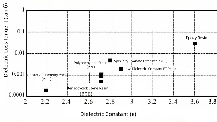
Comparison of Dielectric Properties across various Resin Materials.
> Recommend reading: PTFE/Teflon Dielectric Constant and Its Application in PCBs
Deep Insight: When signal rates escalate beyond 25Gbps, or even reach the 112Gbps standard of 5G-Advanced, the timing jitter caused by the fiber weave effect becomes unacceptable.
| Fiberglass Cloth Specification | Dielectric Constant Fluctuation (Dk Fluctuation) | Impedance Fluctuation Amplitude | Recommended Application Scenarios |
|---|---|---|---|
| Regular Fiberglass (1080/2116) | 0.44 | 2.5 Ω | General industrial, low-speed digital circuits |
| Spread Glass (1067/1078) | 0.18 | 1.0 Ω | 25Gbps+ high-speed transmission |
| NE-Glass (Low-loss glass) | Extremely low | < 1.0 Ω | 110GHz+ RF / AI accelerators |
Expert Recommendation: To mitigate the fiber weave effect, engineers should incorporate a "10-degree angled routing" command into the AI routing script, or request the factory to rotate the circuit image during panelization. Furthermore, specifying the use of spread glass (such as 1078) for critical links is also a mainstream engineering practice.
During the lamination process of a 32-layer PCB, the resin in the prepreg flows into the void areas of the inner layer patterns. This means that Copper Retention directly determines the final dielectric thickness.
If there are large copper-free areas in the inner layers, the loss of resin will cause those regions to become thinner, lowering the transmission line impedance and even triggering risks of inter-layer voids and delamination. NextPCB's engineering team recommends that before conducting signal integrity simulations, the stack-up thickness table must be corrected based on the actual copper retention rate. Using online tools like HQDFM, designers can automatically identify imbalanced copper distributions and manually or via AI add Thieving Copper to ensure thickness consistency post-lamination.
32-layer boards are typically accompanied by extremely complex interconnect structures. With the increase in component pin density (such as 0.4mm pitch BGAs), Any-layer HDI has become a standard specification.
In a 32-layer board, the total depth of through-holes often exceeds 3mm. If the drill diameter is too small, the Aspect Ratio will far exceed 10:1. During the plating process, it is extremely difficult to guarantee the plating thickness at the center of the via hole.
IPC-6012 Class 3 Standard: Requires an average hole wall copper thickness of no less than 20 μm to ensure connection reliability under environmental stress and thermal cycling.
Process Limitations: If the AI-generated aspect ratio exceeds 15:1, manufacturers must employ special plating additives or pulse plating technologies. For medical, aerospace, or automotive electronics projects, engineers must strictly evaluate the factory's aspect ratio limits.
Microvias are the core of HDI. Laser-drilled via diameters typically range from 3-5 mil. To support Via-in-pad technology and prevent voiding during soldering, microvias must undergo electroplating filling.
NextPCB's High-Order HDI Process Metrics:

Micro-section of Solder Joint Voiding induced by HDI Microvia process defects.
As the layer count increases, the internal physical stress of the PCB becomes extremely complex. Failure analysis is no longer just the responsibility of the quality department; it is an engineering variable that must be considered upfront during the DFM stage.
When a PCB undergoes reflow soldering at high temperatures (approx. 260°C), the expansion rate of the resin in the Z-axis is much greater than that of the copper foil. In 32-layer boards, the cumulative effect of this displacement can cause the through-hole copper foil to be torn apart, resulting in barrel cracking.
Expansiontotal = Σi=132 (Thicknessi · CTEz,i · ΔT)
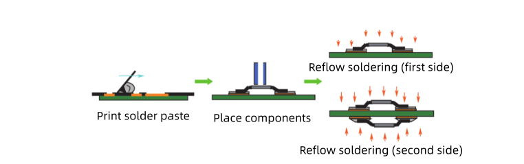
High-temperature Reflow Soldering Environment for High-Order PCB Assemblies.
To tackle this challenge, materials with High Tg (Glass Transition Temperature) and High Td (Decomposition Temperature) must be selected 27. For instance, in the High-Performance Computing (HPC) sector, the commonly used Megtron 6 material features an extremely low Z-CTE (approx. 2.7%), ensuring that vias maintain electrical connection integrity even under multiple thermal shocks.
Under large BGA components on 32-layer boards, mechanical stress often induces micro-cracks in the dielectric layer beneath the pad, a phenomenon known as "Pad Cratering". It is a typical side effect of combining lead-free processes with highly rigid materials.
Mitigation Strategy Checklist:
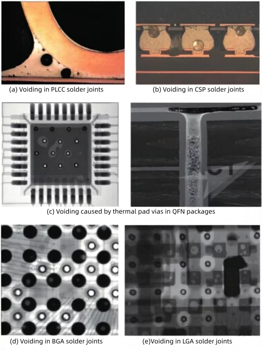
Examples of Solder Voiding across different SMT Package types.
In the dense via arrays of 32-layer boards, the hole-to-hole clearance is extremely small. In high-temperature and high-humidity environments, electrolytic reactions can cause copper ions to grow along the fiberglass bundles, forming Conductive Anodic Filaments and resulting in catastrophic insulation failure.
Expert Recommendation: When designing 32-layer high-density boards, it is recommended to maintain via spacing above 0.4mm and prioritize the use of resin systems with CAF Resistant properties.
As a reliable global electronic manufacturing service provider, NextPCB provides not only manufacturing capabilities but also assists engineers in optimizing 32-layer designs through a digitized MDD workflow.
In high layer count manufacturing, traditional Mass Lam lamination struggles to guarantee inter-layer registration for 32-layer boards due to significant positioning errors. NextPCB employs the PIN Lam system, physically locking each core layer through mechanical pins to ensure inter-layer registration accuracy reaches ±2 mil or even higher. This precision directly determines the control of drill offset, thereby ensuring the integrity of the signal loop.
In ultra-high-frequency designs above 110GHz, signal currents flow only in an extremely thin layer on the surface of the copper foil. If the copper foil surface is rough (high Rz value), the signal transmission path lengthens, resulting in severe resistive losses.
NextPCB offers HVLP2 (Hyper Very Low Profile) copper foil options for AI servers and RF front-end boards:
To reduce R&D iteration cycles, NextPCB has launched the free HQDFM analysis software. This tool not only checks basic DRCs like trace width and spacing but also provides deeper analysis tailored for 32-layer high-order designs:
For high-layer multi-layer PCBs of up to 32 layers, the quality system is not just a certification, but a commitment to process stability.
NextPCB has obtained the IATF16949:2016 quality management system certification. Although this standard was originally designed for the automotive industry, its core philosophy—defect prevention, reduction of variation, and waste reduction in the supply chain—has immense universal applicability for highly complex 32-layer HDI boards.
> Browse all our certificates: NextPCB Promise the Product Safety with ISO 9001 UL Certifications - NextPCB
When producing 32-layer high-order PCBs, IATF16949 requires:
In the industrial, medical, and aerospace sectors, IPC Class 2 is often insufficient to meet demanding mission requirements. NextPCB supports manufacturing to the IPC Class 3 high-reliability standard :
To assist engineers in ensuring the success rate of their designs prior to file release, the following table summarizes the critical DFM verification dimensions for 32-layer high-order PCBs.
| Checklist Item | Engineering Focus | Recommended Standard |
|---|---|---|
| Stack-up structure symmetry | Prevents board warpage during reflow soldering | Dielectric layers and copper thickness must be symmetrical about the central axis 21 |
| Copper retention balance | Ensures uniform pressing pressure and impedance consistency | Single-layer copper retention difference controlled within 20% 21 |
| Via Antipad | Reduces via parasitic capacitance, optimizes return paths | Use elliptical or oversized antipads for differential pair vias 29 |
| Backdrill depth | Eliminates signal resonance caused by long via stubs | Stub length should be controlled within 5 mil (0.127mm) 1 |
| Minimum inter-layer thickness | Prevents short circuits caused by CAF or dielectric breakdown | Prepreg between signal and ground layers is not recommended to be less than 2.5 mil 11 |
| High-frequency hybrid stack-up | Balances cost and performance (e.g., Rogers + FR4 hybrid) | Focus on adhesion and CTE matching at the hybrid interface 21 |
| Thermal Vias | Solves high power dissipation issues of ASICs/GPUs | Place 0.2mm blind via arrays under the bottom thermal pad 14 |
The PCB industry is entering a brand new era defined by AI algorithms and realized through physical processes. In the development of 32-layer high-order PCBs, any digital optimization that ignores the realities of physical tolerances will be castles in the air. By deeply integrating the "Manufacturing-Driven Design (MDD)" concept with AI design automation, engineers can predictively resolve pain points such as impedance fluctuations, inter-layer failures, and signal losses.
Leveraging its profound IATF16949 quality heritage, PIN Lam precision lamination system, and HQDFM digital toolchain, NextPCB is dedicated to becoming the best bridge for global hardware engineers to cross the "digital-to-physical" chasm. For projects pursuing ultimate performance and long-cycle reliability (such as 5G base stations, AI servers, or high-performance industrial computers), choosing a partner with engineering insight is far more important than choosing a simple processing factory.
Your Action Guide:
In the future of the Internet of Everything and computing power explosion, every 32-layer microscopic world will become a solid cornerstone supporting digital civilization.
While traditional autorouters often created inefficient "spaghetti" layouts, modern AI-Driven Design (like Allegro X AI) utilizes physics-aware algorithms. In 32-layer boards, where manually managing thousands of microvias and differential pairs is nearly impossible, AI can optimize for Signal Integrity (SI) and Power Integrity (PI) in hours rather than weeks, ensuring paths meet strict electromagnetic field requirements.
At ultra-high frequencies (112Gbps and 224Gbps), the Skin Effect forces current to flow only on the very surface of the copper. If the surface is rough (high Rz value), the signal must travel up and down the "peaks and valleys," increasing the path length and resistive loss. Using HVLP2 (Hyper Very Low Profile) copper is essential to keep the surface mirror-smooth and minimize insertion loss.
The risk is real. Because resin expands much more in the Z-axis than copper does when heated to 260°C, the thick stack-up of a 32-layer board acts like a mechanical piston, stretching the vias. This can lead to Barrel Cracking. To prevent this, engineers must specify High-Tg materials and ensure copper wall thickness meets IPC Class 3 standards (minimum 25μm) to withstand the thermal stress.
Standard DFM is often a "post-mortem" check—you send files to the factory, and they tell you what's broken. MDD is proactive; it integrates factory-specific tolerances (like Etch Factors and press-out thicknesses) directly into the AI design phase. Using tools like HQDFM, you simulate the manufacturing reality before the board is even made, significantly reducing the need for costly redesigns (re-spins).
Yes. While 10-degree angled routing is effective, it can make a 32-layer layout very messy. A more industry-standard engineering solution is specifying Spread Glass (e.g., 1067 or 1078) in your BOM. These fabrics are woven more tightly and flatly, eliminating the "gaps" between fibers and providing a uniform Dielectric Constant (Dk) across the entire board, which is vital for maintaining timing at speeds over 25Gbps.

Still, need help? Contact Us: support@nextpcb.com
Need a PCB or PCBA quote? Quote now

