
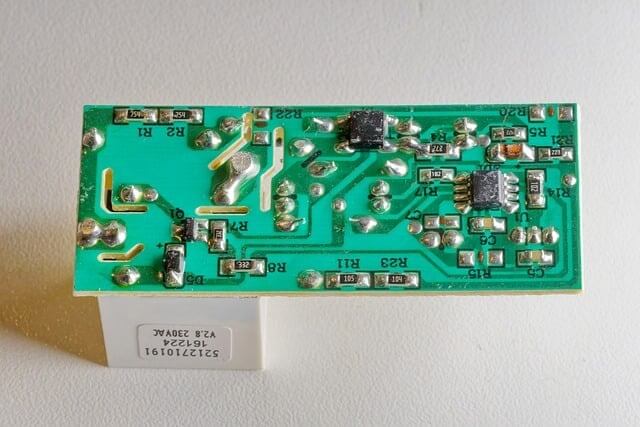
 PCB Assembly
 Layer Buildup
 Online Tools
 PCB Design-Aid & Layout
 Mechanics
 SMD-Stencils
 Quality
 Drills & Throughplating
 Factory & Certificate
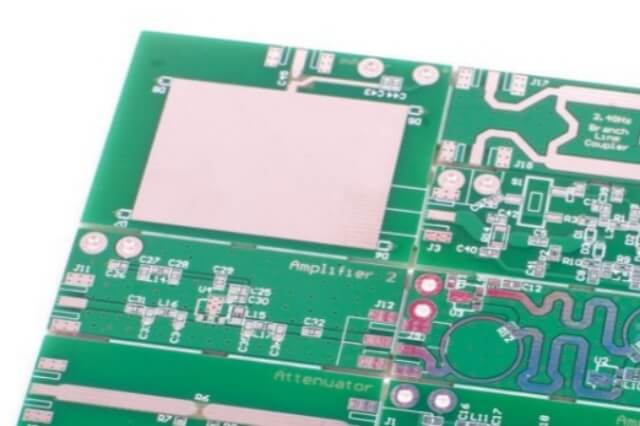
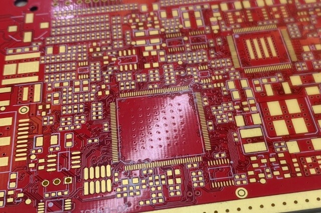
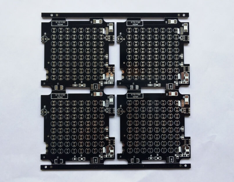
 PCB Assembly Factory Show
Certificate
PCB Assembly Factory Show
Certificate
Support Team
Feedback:
support@nextpcb.com


Introduction
A Printed Circuit Board (PCB) is the fundamental nervous system of virtually every modern electronic device – the rigid or flexible platform providing crucial mechanical support and intricate conductive pathways, typically using etched copper traces. From simple LED printed circuit boards to complex aerospace computers, PCBs form the foundation of electronic innovation. Understanding the different types of PCB boards is not just academic; it's critical for engineers and designers to select the optimal circuit board type ensuring performance, reliability, manufacturability, and cost-efficiency. This definitive guide explores the primary classifications, common applications, benefits, and selection criteria – empowering you to choose the perfect PCB board for your next project.
PCBs are categorized based on several key characteristics, each with significant design and performance implications:
Structure: A single layer of copper traces laminated onto one side of an insulating rigid substrate (like FR-2 or CEM-1). Electronic components are placed and soldered only on the copper side.
How It's Made: The most basic fabrication using etching or older methods like screen-printing or photoresist.
Common Uses: Extremely simple electronics: Basic calculators, LED lighting boards, power supplies for small appliances, toys, timing circuits.
Pros:
Cons:
Structure: Copper layers laminated onto both sides of an insulating substrate. Traces on both sides are interconnected electrically through Plated Through-Holes (PTHs), or vias.
How It's Made: Similar etching/photolithography as single-sided, plus drilling and plating processes to create conductive holes. Standard FR-4 material dominates.
Common Uses: Power supplies, instrumentation, HVAC controllers, automotive dashboards, moderate complexity audio gear. Ubiquitous for IoT devices with more features than single-sided allows.
Pros:
Cons:
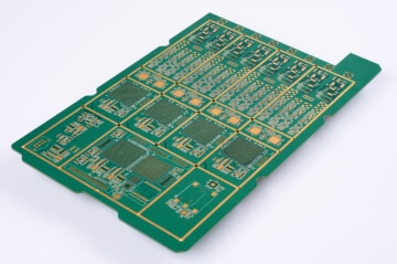
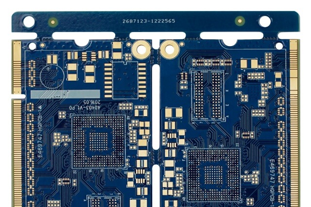
Structure: Three or more conductive copper layers, separated by insulating prepreg (pre-impregnated fiberglass) layers, laminated together under heat and pressure into a single, unified board. Internal layers often serve solely as dedicated power or ground planes. Complex interconnection is achieved using vias (through-hole, blind, buried).
How It's Made: Complex laminated stack-up, precision layer alignment, advanced drilling for microvias in HDI, multiple cycles of lamination/etching.
Common Uses: The backbone of modern computing and communication: Motherboards, smartphones, networking equipment (routers, switches), medical instruments, aerospace avionics, sophisticated industrial controls, automotive engine control units (ECUs). Crucial for PCB types for automotive and medical devices demanding reliability and compactness.
Pros:
Cons:
Typical Layers: 4, 6, 8, and 12 layers are common; high-end designs can reach 32, 64, or even more layers for massive complexity (like server boards).
Definition: The most prevalent type of PCB. Made from solid, inflexible substrate material (overwhelmingly FR-4 glass epoxy resin).
Common Substrates: FR-4 (standard), FR-4 High-Tg (for higher temperature resistance), CEM-1, CEM-3, specialized RF PCB materials like PTFE/Rogers®.
Use Cases: Found in virtually all electronics requiring a stable platform: Computers/motherboards, TVs, industrial control systems, GPS modules, medical instruments, automotive dashboards and ECUs. Ideal for applications with no need for bending or shape conformity.
Key Attributes:
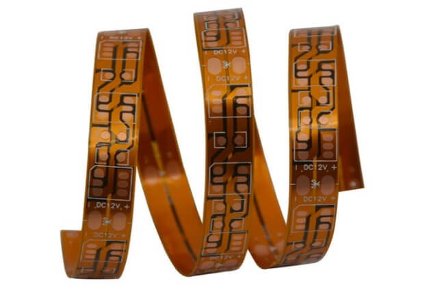
Substrate: Flexible plastic films like polyimide or polyester (PET). Conductive traces are typically rolled annealed copper, etched onto the flexible substrate.
Connections: Achieved via flexible layer-specific vias or termination points (pads/fingers).
Advantages:
Design Variations: Available as single layer PCB board, double-sided PCB, or even multilayer PCB board.
Common Uses: Wearables (smart watches, fitness trackers), flexible displays, camera modules, medical probes/implants, dynamic components (printer heads, robot arms), tight spaces within consumer electronics, intricate automotive sensor arrays.
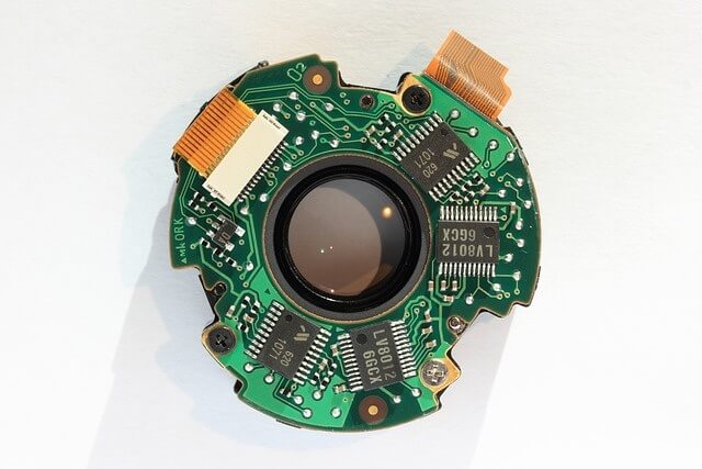
Hybrid Approach: Combines multiple layers of rigid PCB material with layers of flexible PCB material bonded together as a single, integrated structure. Provides both stable mounting areas for components and dynamic interconnections.
Structure: Rigid sections (with components) connect via integrated flexible sections (with traces). Flexible layers usually continue into the rigid areas seamlessly ("coverlay" or "covercoat" on flex replaces soldermask). Requires sophisticated lamination cycles.
Ideal For:
Benefits:
Core Features: Characterized by ultra-fine geometry: Microvias (diameters ≤150µm, typically ≤100µm in advanced), blind/buried vias (used in conjunction with traditional through-vias), thinner traces/spaces ≤100µm. Often employs stacked or staggered microvias and laser drilling technology. Can be either rigid PCBs or rigid-flex PCBs.
Optimized Applications: Smartphones & tablets, compact wearables, miniaturized medical devices, high-speed digital designs (servers, networking backplanes), BGA breakout routing for fine-pitch chips. The best PCB type for ultimate density.
Key Drivers & Considerations:
Structure: The dielectric layer (special thermally conductive material) is bonded to a metal baseplate/heat spreader (typically aluminum, sometimes copper – forming a copper PCB, or more rarely iron alloys/ceramic matrix). Conductive layer(s) on top. Often single-sided or double-sided.
Why the Metal Core? Excellent thermal dissipation. The metal baseplate sucks heat away from power components (LEDs, motor drivers, power transistors, regulators).
Primary Applications: LED lighting systems (where it's arguably the best PCB type for LED lights), power supplies/converters, power electronics, motor controllers (especially PCB types for automotive), automotive headlights, solid-state relays. Ideal where conventional PCB material like FR-4 struggles thermally.
Key Benefits: Dramatically increases thermal performance, manages thermal expansion mismatch better than FR-4 with power components, improves reliability.
Mission Critical: Maintaining signal integrity and minimizing dielectric signal loss and distortion at microwave frequencies (>1 GHz) and RF is paramount.
Substrates: Engineered for stable electrical properties. Common materials include:
PTFE Composites (Rogers®, Taconic®, Isola AstraMT77): Excellent high-frequency performance and low loss.
Properties Required: Tightly controlled dielectric constant (Dk) and dissipation factor (Df), low moisture absorption, dimensional stability over temperature.
Applications: Telecommunications (5G/6G antennas, filters, amplifiers), radar systems, satellite communications, high-speed signal processors. Essential in RF PCB amplifiers and satellite modules.
Heavy Copper PCBs:
High-Tg PCBs:
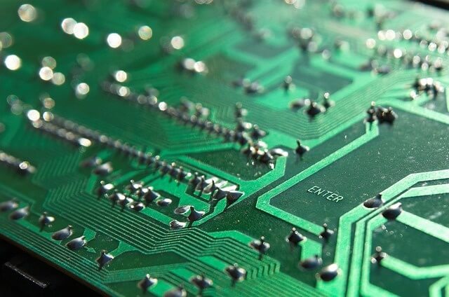
This term typically refers to conventional PCBs manufactured via subtractive etching of copper on laminates using photoresist imaging/photolithography or screen printing. It encompasses the vast majority of single-sided, double-sided, and multilayer PCB boards discussed previously. The 'graphical' aspect stems from the creation of the trace pattern using imaging techniques. Almost all modern mainstream PCBs fall into this category unless specified otherwise (like the types below).
|
PCB Type |
Layers |
Flexibility |
Common Applications |
Key Benefits |
Material/Primary Drivers |
|
Single-Sided |
1 |
Rigid |
Simple LEDs, calculators, timers, power supplies (low watt) |
Lowest cost, easy design/manufacture |
FR-1/-2, CEM-1 |
|
Double-Sided |
2 |
Rigid |
Power supplies, amplifiers, automotive dashboards, IoT sensors |
Good cost/performance, increased density over single-sided |
FR-4 (standard) |
|
Multilayer |
4-32+ |
Rigid |
Motherboards, smartphones, telecom/networking, automotive ECUs, medical |
Highest density, superior signal integrity, embedded power/ground planes |
FR-4 (std/high Tg), Polyimide |
|
Flex |
1-Multilayer |
Flexible |
Wearables, cameras, foldables, robotics, dynamic cabling |
Bendable, space-saving, lightweight, vibration/shock resist |
Polyimide/Kapton®, PET |
|
Rigid-Flex |
Multi |
Hybrid (Rig/Flex) |
Aerospace/defense systems, complex consumer devices (foldable), medical implants |
3D design freedom, reliability (reduced connectors), space/weight sav |
FR-4 + Polyimide |
|
HDI |
4-32+ |
Often Rigid |
Smartphones, ultra-miniature devices, high-speed digital BGA breakout |
Microvias, ultra-fine features, maximum density, improved RF perf |
FR-4, Polyimide, RF materials; Laser drilling |
|
Metal-Core |
1-2 |
Rigid |
LED lighting, high-power electronics, motor drivers, BMS |
Exceptional thermal dissipation, power delivery strength |
Aluminum base (IMS), Thin dielectric |
|
RF/High-Freq |
Varies |
Rigid (usu.) |
Antennas, RF amplifiers, 5G/6G telecom, satellite modules |
Controlled impedance, minimal signal loss, stable Dk/Df |
PTFE (Rogers®), Ceramic composites |
|
Heavy Copper |
Varies |
Rigid |
Power converters, welding, industrial motor controllers |
Handles very high currents, robust power paths |
Thick base copper foils (4oz+), Robust soldermask |
|
High-Tg |
Varies |
Rigid |
Automotive under-hood, high-temp industrial equipment |
Resists warping at high temp, reliability in harsh environments |
High-Tg FR-4 (170°C+), Polyimide, Ceramic composites |
|
Discrete-Wire |
Varies |
Rigid |
Obsolete: Historical prototypes, specialist legacy |
Custom wiring, robustness |
N/A (legacy technique) |
Selecting the ideal types of circuit board involves balancing key factors:
Complexity: How many components? How complex are the interconnections? (Single/Double vs Multi/HDI).
Performance:
Mechanical: Need to bend or fold? Install in complex 3D shape? (Flex/Rigid-Flex). Stable structure? (Rigid)
Substrate: FR-4? High-Tg FR-4? Polyimide for flex or high-temp? RF materials? Aluminum core?
Copper Thickness: Standard 1 oz? Heavy Copper (2-20+ oz)? Impacts current capacity, heat dissipation.
Surface Finish: HASL, ENIG (gold), Immersion Silver/Tin? Affects solderability, cost, reliability.
Recommend Reading: HASL vs ENIG: An Ultimate Guide on Surface Finish
Layer Count: What do you genuinely need? Unnecessarily high layers increase cost/time.
Technology Level: Can you design/build with Microvias (HDI)? Complex Rigid-Flex stackups?
Feature Limits: Minimum trace width/space size? Via drill sizes? Microvia capability?
Testing Requirements: Simple bare-board testing? Complex in-circuit (ICT) or functional testing (FCT)? Required for rigorous PCB quality.
Lowest Cost: Single-sided wins, but with functionality limits.
Best Value: Double-sided often offers the best performance-to-cost ratio for mid-complexity.
Premium Performance: Multi-layer, Flex, Rigid-Flex, HDI deliver high density/integrity at a premium price. Forced by complexity/performance requirements.
Thermal/Power: Metal Core adds cost, essential if heat is the primary challenge.
Partnering with an experienced manufacturer like NEXTPCB is crucial. Select a partner who offers:
Whether your project demands the simple cost-efficiency of a single-sided LED printed circuit board or the advanced capabilities of HDI rigid-flex for aerospace electronics, understanding and selecting the correct types of PCB board is fundamental. It dictates the electrical performance, thermal management, form factor, reliability, and ultimately, the success and cost of your product.
Don't design in the dark! Leverage this comparative knowledge of circuit board types to make an informed foundation decision. Explore the extensive PCB technology capabilities and free DFM resources on platforms like NEXTPCB. Utilize their instant online quote system and expert engineering support to transform your concept into a perfectly manufactured reality. Request your free PCB quote today – build your electronics on the right foundation.
1. Q: What are the most common types of PCBs? How many exist?
2. Q: What is a Printed Circuit Board actually made of?
3. Q: Rigid vs. Flexible PCB: When to choose which?
4. Q: Multilayer vs. HDI PCB - what's the key difference?
A: While HDI PCBs are a subset of multilayer PCBs, they specifically utilize advanced miniaturization technologies:
5. Q: Are Aluminum PCBs more expensive than FR-4? Why use them?
A: Yes, Metal-Core PCBs (Aluminum-Backed) are typically more expensive per unit area than a standard FR-4 PCB of the same layer count and size. However, they are chosen primarily for overcoming thermal limitations. If a design generates significant heat (like high-power LEDs or motor drivers), the thermal management benefits of the metal core can significantly improve performance, prevent failure, increase longevity, and can even reduce net system cost by eliminating expensive heatsinks or complex forced air cooling required with FR-4. The thermal dissipation is the key payback.
6. Q: Can you provide printed circuit board examples for different industries?
A:
7. Q: What does substrate choice mean for thermal handling?
A: Different PCB materials have vastly different abilities to conduct heat:
Choosing the right substrate is crucial for designs generating heat. A poor thermal substrate traps heat near components, reducing reliability and performance. Aluminum-core dielectrics and strategic thermal via placement are the main tools for actively managing heat through the substrate beyond copper pours.
8. Q: I'm new to PCB engineering - how do I start choosing?
A: Understand your core requirements (Step 1, Section 7). For low-cost, simple circuits (a few LEDs, a timer IC, low voltage/current), single-sided suffices. Adding moderate complexity (microcontrollers, moderate power) usually demands double-sided. High complexity or speed needs lead to multilayer. If things need to bend or fit unusually, research flex. Significant heat? Look at metal-core. High-frequency signals? RF materials matter. Simplify as much as possible initially. Collaborating with a knowledgeable PCB manufacturing partner early (like requesting DFM checks and discussing your goals with vendors such as NextPCB) is invaluable for beginners navigating these types of circuit board choices and PCB board uses. Don't underutilize their expertise! Consider quick turn PCB types for prototyping designs.
Resources Recommended
Free HQDFM Tool: Validate Designs in Seconds
Download Advanced PCB Material Selection Guide (FR4, Polyimide, Rogers®)
Still Decoding PCB Types? Consult Our Engineers
Still, need help? Contact Us: support@nextpcb.com
Need a PCB or PCBA quote? Quote now


 Printed Circuit Boards
 Surface

