
 NextPCB Capabilities
Printed Circuit Boards
NextPCB Capabilities
Printed Circuit Boards
 PCB Assembly
 Layer Buildup
 SMD-Stencils
 PCB Design-Aid & Layout
 Mechanics
 Quality
 Drills & Throughplating
 Factory & Certificate
 PCB Assembly Factory Show
Certificate
PCB Assembly Factory Show
Certificate
Support Team
Feedback:
support@nextpcb.com


Last reviewed: [MONTH YEAR] | Reviewed by the NextPCB engineering content team
In short: IPC classes are a three-tier system—Class 1, Class 2, and Class 3—defined primarily under IPC-A-610 (and referenced in IPC-6011/6012 for bare boards) that classify a PCB or PCB assembly by how critical its reliability and defect tolerance need to be, ranging from general consumer electronics (Class 1) to mission-critical aerospace and medical hardware (Class 3).
In the electronic interconnection industry, IPC stands as the global trade association. The primary goal of the IPC Class system is to standardize the assembly, production processes, and quality requirements of electronic components. Established in 1957 under the name Institute of Printed Circuits, it later transitioned to the Association Connecting Electronics Industries.
The organization publishes specifications and requirements regularly. Adhering to the IPC standard is one of the most accepted protocols in the global electronic industry. These standards provide hardware engineers and procurement teams with a unified baseline to design, fabricate, and test reliable, high-quality PCB products.
IPC outlines three major classes of PCBs governed under IPC-6011. Every class explains the board types, performance expectations, and the acceptable number of defects. The significant difference between these three classes is the degree of inspection through which electronic assembly should go.
The Class 1 board is referred to as the general electronics board. Manufacturers design these for applications where the primary requirement is the function of the completed assembly. They allow various cosmetic and minor structural defects as long as it doesn't affect the board's immediate functionality. Reliability is not a significant factor here. Engineers specify Class 1 for products with short life spans, primarily everyday consumer electronics and toys.
Class 2 boards deliver higher reliability and an extended life expectancy compared to Class 1. They follow a more specific standard but still allow some cosmetic imperfections. Products using Class 2 PCBs expect uninterrupted service, but absolute failure-free operation is not highly critical. You will find these boards implemented in laptops, tablets, communication equipment, and standard industrial control systems.
Class 3 represents the highest commercial quality standard. Equipment operating under this class must provide continuous, uninterrupted performance on demand. Downtime cannot be tolerated. The board goes through an aggressive level of inspection and testing, following precise tolerances in board design. Applications encompass life support systems, automotive engine controls, military equipment, and aerospace electronics.
Boards in Class 2 are more accessible and faster to inspect than those in Class 3. The specific rules governing a Class 3 component increase optical and X-ray inspection time significantly. Comparatively, the inspection process for Class 2 boards is efficient, keeping production moving. For Class 3, meticulous assessment identifies deficiencies before complete creation, guaranteeing that the high-performing hardware earns the clients' absolute trust.
The manufacturing of Class 3 boards takes a significantly longer time because fabrication facilities must slow down certain chemical and mechanical processes—like copper plating—to ensure perfection. This tight process control increases expenses. Class 2 maintains a steady manufacturing rhythm, making it the ideal baseline for an efficient quick turn PCB run.
During the layout of Class 3 boards, engineers exercise a zero-tolerance policy for specific defects and adhere to strict geometric specifications. In contrast, Class 2 PCBs offer designers more breathing room. It is structurally simpler to place and route components when routing density rules align with standard Class 2 tolerances.
The divergence between Class 2 and Class 3 becomes highly apparent during the PCB assembly phase. Differences surface in plating thickness, component placement accuracy, chemical cleanliness, and specific protocol requirements.
During the SMT assembly process, component leads can be slightly off the pad. If the overhang does not compromise the mechanical strength or electrical performance of the joint, Class 2 accepts this visual defect. However, Class 3 inspectors will fail the assembly for the same misalignment. Class 3 accepts zero imperfections that might degrade under thermal cycling.
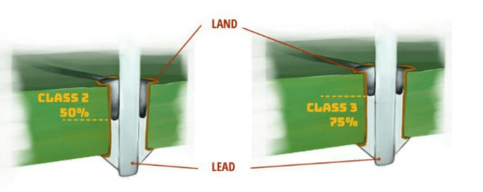
The volume of solder inside a Plated Through-Hole (PTH) is a defining metric. For Class 2, the acceptable amount to fill the barrel for a through-hole lead is 50%. Class 3 requires a massive 75% barrel fill to ensure mechanical rigidity under heavy vibration. Getting the proper amount of solder paste into the smaller plated holes without causing bridging is a delicate thermal profile process during wave soldering.
| Assembly Characteristic | IPC Class 2 Requirement | IPC Class 3 Requirement |
|---|---|---|
| Surface-mount components | Can be slightly placed off the pad (if it doesn’t affect electrical/mechanical performance). |
|
| Barrel Fill (PTH) | Through-hole leads require 50% fill. | Through-hole leads require 75% fill. |
| Characteristics | Class 2 | Class 3 |
|---|---|---|
| Circular wetting of solder on lead and plated holes (component side) | 180° | 270° |
| Circular wetting of solder on lead and plated holes (solder side) | 270° | 330° |
| Plated Through Hole fill | 50% | 75% |
| Land Area covered with solder on the solder side | 75% | 75% |
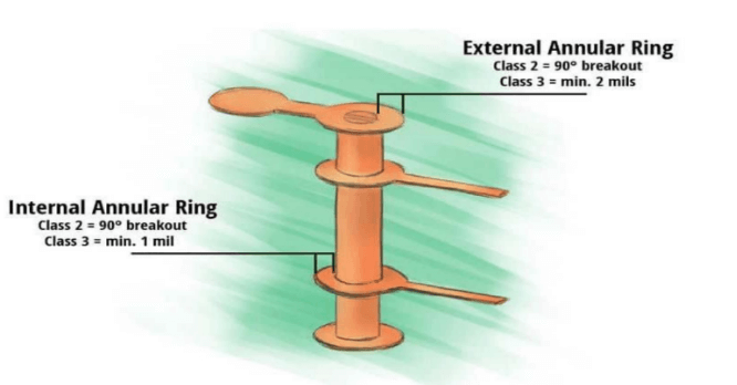
Drill breakout directly impacts the structural integrity of vias. During fabrication, the drill bit might slightly deviate from the exact pad center. Class 2 accepts a 90-degree breakout of the hole, provided it maintains the minimum lateral spacing. In Class 3, any breakout is strictly forbidden. Class 3 boards mandate an unbroken annular ring to guarantee high reliability under mechanical stress.
The minimum dielectric requirement for both Class 2 and Class 3 stands at 3.5 mils. Users and suppliers must negotiate specific dielectric materials based on impedance control needs. While standard FR4 works perfectly for most Class 2 designs, Class 3 applications involving high frequencies or extreme temperatures often require advanced base materials like high-Tg FR4 or Rogers laminates.

The extensive testing, slower plating times, and zero-defect tolerances required for a Class 3 assembly product can add up to 20% to the total product cost. Furthermore, a higher concentration of through-hole components naturally increases the manufacturing expenses of the Class 3 board due to manual intervention or specialized wave soldering setups.
If you are developing standard IoT or commercial hardware, specifying Class 2 is a highly effective way to secure a low cost PCB without sacrificing functionality. Partnering with a capable fabricator like NextPCB for turnkey PCB services ensures that whether you require rapid prototyping or full-scale Class 3 medical board production, your Bill of Materials (BOM) and fabrication processes are optimized for maximum yield.
To prevent fabrication bottlenecks, hardware engineers must integrate Design for Manufacturability (DFM) guidelines early in the layout phase:
PCB-related standards formulated by the IPC define what makes a board acceptable or defective. Standard IPC-A-600 covers bare board acceptability, while IPC-A-610 dictates the standards for electronic assemblies. Any manufacturer or electronics designer must comply with IPC, as these standards are the most widely accepted worldwide.
Annular Ring Defects
Copper pads surround drilled holes, creating the annular ring. Annular ring breakout is an IPC PCB defect commonly found during bare board inspection. It remains a primary concern for high-vibration applications. As established, Class 2 allows up to 90 degrees of fracture, but Class 3 outright rejects it.
Solder Joint Defects
Cold solder joints occur when there is inadequate heat transferred to the pad. Sometimes, this happens if the soldering iron runs at a shallow temperature or the reflow profile cools too rapidly. These defects compromise the electrical connectivity of the PCB. Applying the correct thermal profile is the only way of avoiding such problems.
Component Misalignment
Misalignment takes place when components float on molten solder during the reflow stage—often due to imbalanced pad dimensions or excess paste. IPC dictates specific overhang rules. The acceptable misalignment limit relies on pad width reduction, with Class 3 permitting significantly less variance than Class 1 and Class 2.
Need Precise Thresholds? Choosing between Class 2 and Class 3 affects tolerances across design, fabrication, and assembly. Instantly check the specific class requirements for your target standards on our comprehensive IPC Standards Classes Hub.
The main difference is the tolerance for manufacturing defects and component alignment. Class 3 boards are built for critical applications and require uninterrupted performance, meaning they have strict zero-breakout rules for annular rings and require 75% barrel fill. Class 2 allows slight cosmetic defects and 50% barrel fill for dedicated service electronics.
It depends on the device classification. You can use Class 2 for non-critical medical monitoring equipment. However, life-support systems, implantable devices, or critical diagnostic hardware require IPC Class 3 to ensure absolute reliability and safety.
Manufacturing a Class 3 board typically costs 15% to 20% more than a Class 2 board. The cost increase stems from slower plating processes to achieve thicker copper, rigorous AOI/X-ray inspections, and tighter material yields due to lower defect tolerances.
IPC dictates the proper standards and protocols for manufacturing, designing, and testing your circuit boards. Selecting the exact class ensures you do not over-engineer a simple consumer product or under-spec a critical automotive module. By evaluating the assembly differences, barrel fill logic, and DFM rules, you can optimize your next project for the perfect balance of cost and reliability.
If you need expert assistance determining the exact IPC specifications for your hardware, or if you are ready to start production, do not hesitate to contact us. NextPCB offers industry-leading capabilities to handle both standard and high-reliability fabrication runs.
Explore More IPC Standards:
Still, need help? Contact Us: support@nextpcb.com
Need a PCB or PCBA quote? Quote now


 Surface

