NextPCB Capabilities
Printed Circuit Boards
NextPCB Capabilities
Printed Circuit Boards
 PCB Assembly
 Layer Buildup
 SMD-Stencils
 PCB Design-Aid & Layout
 Mechanics
 Quality
 Drills & Throughplating
 Factory & Certificate
 PCB Assembly Factory Show
Certificate
PCB Assembly Factory Show
Certificate
Support Team
Feedback:
support@nextpcb.com


Introduction
Printed circuit board (PCB) basics start with the single-layer PCB—also called a single-sided or 1-layer board—featuring one copper layer on an insulating substrate. prized for simplicity, fast turnaround, and low cost, these boards remain common in consumer electronics, industrial control, and simple power modules even as multilayer designs grow. This guide explains what single-layer PCBs are, their stack-up, key design rules and DFM, manufacturing steps and finishes, cost drivers, and typical applications—so you know when a 1-layer board is the right fit and how to build it correctly.
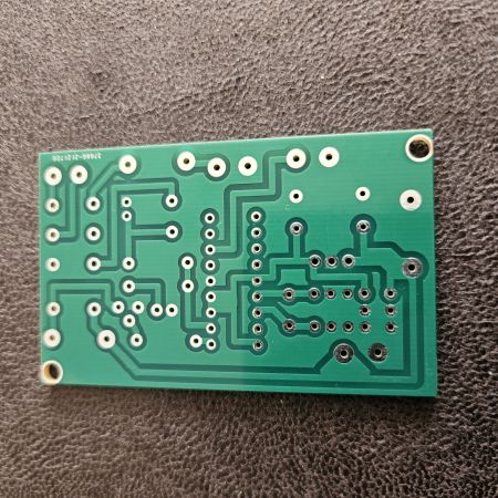
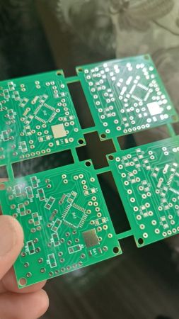
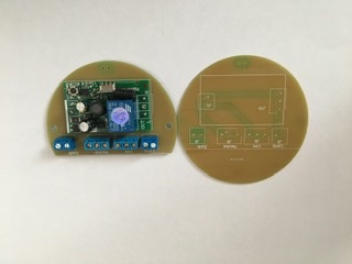
Single Layer PCB ( also called Single sided PCB or 1 layer PCB) is named for its single layer of conductive patterns. While multilayer PCB technology is increasingly popular, single layer PCBs remain widely used due to their unique advantages. They are not only structurally simple and cost-effective but also extremely reliable in specific fields. Below, we will delve into 1 layer PCBs, covering their basic structure, design and manufacturing processes, common applications, and future development trends.
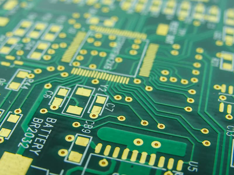
1 layer PCBs are not as complex as they might seem; their biggest feature is their simple structure. They mainly consist of the following layers:
Compared to multilayer PCBs, single-sided ones have distinct advantages: low cost, quick design and manufacturing, and decent heat dissipation. However, they also have drawbacks; with only one layer of routing space, they cannot accommodate very complex circuits and may face challenges in signal transmission and interference resistance.
Despite their simple structure, the design of single sided PCBs requires careful consideration to ensure circuit performance and manufacturability.
This is the starting point for all PCB designs. The most important aspect is selecting the right components and ensuring they have corresponding package libraries in the design software. Power and ground lines are the "lifelines" of the circuit; on a single layer board, we usually create a ground plane by using a large area of copper, which effectively lowers resistance and reduces noise. Critical signal lines should be kept short and away from interference sources, and filtering may be necessary.
This part poses the biggest challenge in single-sided design and must follow several core principles:
○Trace Width and Spacing: Trace widths should be determined based on current size to ensure they can handle adequate current. Sufficient spacing should be left between traces to prevent short circuits.
○ Corner Treatment: When routing turns, it's best to use 45-degree angles or arcs instead of right angles, as right angles can cause signal reflections.
○ Power and Ground Lines: In addition to copper pour, star grounding can be used to prevent ground loops and noise generation.
There are various PCB design software available, such as Altium Designer, Eagle, and KiCad. Choose the one you are most comfortable with and accustomed to.
While the single layer PCB manufacturing process is simple, each step must be strictly controlled to ensure final quality.
Manufacturing Process
○ HASL: Cost-effective but may not provide a very flat surface.
○ ENIG: Provides a very flat surface, suitable for components requiring fine soldering.
○ OSP: Eco-friendly and lower cost, but has a relatively shorter shelf life.
How much does a single PCB cost? Single layer PCBs cost usually range from $0.1 to $5 for quick-turn with Fr-4 material. To understand the 1 layer PCB price, we can mainly analyze it from two core factors: PCB materials and PCB processing technology. These two factors together determine its low price.
The first is the material cost. Single layer PCBs only cover copper foil on one side of the substrate, while double-layer or multi-layer boards need to be stacked between multiple layers. This single-sided structure greatly reduces the demand for key raw materials such as copper foil and insulating materials, fundamentally reducing material costs.
The second is the processing cost. The production process of single sided PCB is relatively simple. Since only one side needs to be wired and etched, the factory does not need to deal with complex inter-layer alignment, multi-layer lamination or buried vias. The simple process not only improves production efficiency, but also reduces the error rate, thereby reducing labor and equipment costs.
Therefore, the low-cost advantage of 1 layer PCB mainly comes from its streamlined material usage and simplified manufacturing process.
Want to know all the factors that affect PCB Cost? Click to view the in-depth analysis article: "Custom PCB and PCBA Cost Analysis: How to Optimize Design and Reduce Expenses".
The final price is determined by your Gerber files.
| Specifications | Capability |
| PCB Material | Fr-4/Aluminum/Copper/Flexible Boards |
| Size | 10mm to 600mm |
| Quantity | 5pcs - 100000pcs |
| PCB Thickness | from 0.6mm to 3.2mm, usually 1.6mm |
| Solder Mask Color | Green/Red/Yellow/Blue/White/Black/Matte Black |
| Silkscreen | White/Black |
| Outer Copper Weight | 1oz to 2oz |
| Trace Width/Spacing | 3.5mil to 10mil |
| Min. Drill Hole | 0.15mm/0.2mm/0.25mm/0.3mm/others |
| Via Processing | Tented Vias/Open Vias/Solder Mask Plug/Via in Pad |
| Surface Finish | HASL/Lead-free HASL/ENIG/OSP |
| IPC Class Level | IPC Class 2 & 3 |
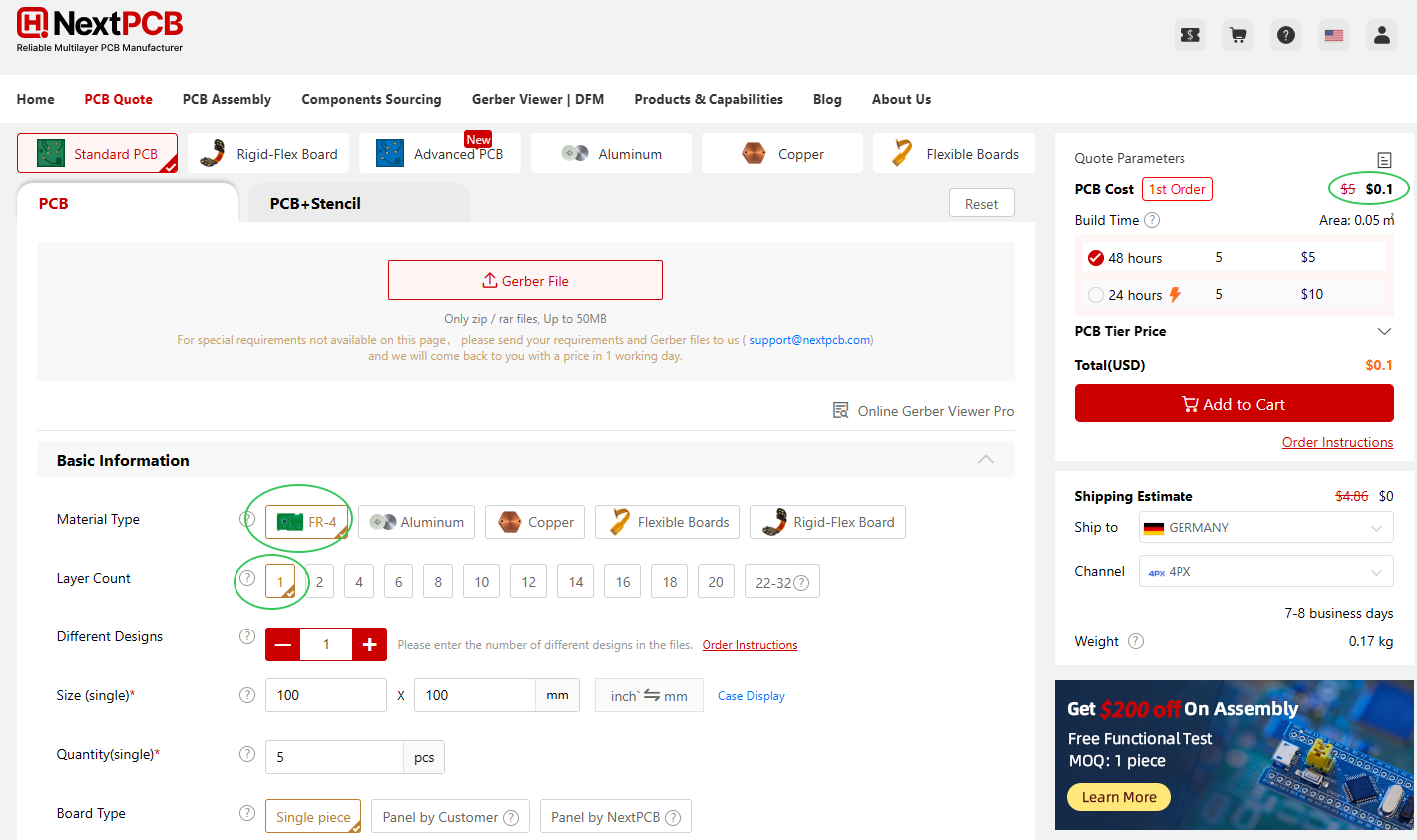
Get Single Layer PCB Cost Online
Thanks to their low cost and quick manufacturing, single layer PCBs have become the preferred choice for many simple electronic products.
Despite facing competition from multilayer boards, single layer PCBs continue to evolve, with numerous future opportunities.
In summary, single layer PCBs hold an irreplaceable position in the electronics industry due to their cost advantages, ease of manufacturing, and reliability. Although single sided PCBs are less complex than multilayer boards, they remain the preferred solution in many consumer electronics, industrial control, and simple power applications. With continuous innovation in materials and manufacturing technologies, as well as the driving force from emerging fields like IoT, single layer PCBs will continue to play a key role in meeting the ever-changing market demands.
Want to learn about the single sided PCB assembly process? Our comprehensive guide, 《PCB Assembly - A Comprehensive Guide》, provides the detailed information you need. Whether you are beginners or experts, you'll find valuable insights here.
Your best alternative for PCB manufacturing and assembly. We balance quality and cost, striving to provide high-value, competitive solutions for your projects. We're more than just a service provider, we're your strategic partner. From prototype to mass production, we offer efficient, precise, one-stop services, providing strong support for your project.
You may also be interested in...
2 Layer PCBs: A Complete Guide to Production, Pricing, and Applications
Multilayer PCBs: A Comprehensive Guide to Design, Manufacturing, and Applications
Still, need help? Contact Us: support@nextpcb.com
Need a PCB or PCBA quote? Quote now


 Surface