Introduction: It's Not Just About "Melting"
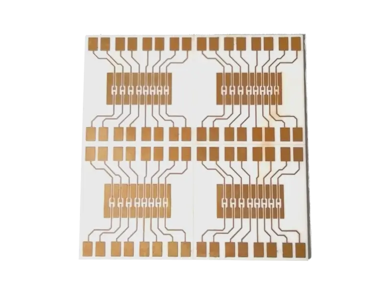
If you are designing a 2-layer prototype for a hobby project, standard FR-4 is perfectly adequate. But as professional engineers move toward high-layer counts, lead-free assembly, and harsh operating environments, a standard board often becomes the weakest link in the reliability chain.
A common misconception is that a PCB fails because it "melts." In reality, failure is often silent and invisible from the outside. The culprit is usually the Glass Transition Temperature (Tg) and the mechanical stresses that occur when that threshold is crossed.
For PCB designers, the choice between High Tg PCB and Standard FR4 is a balancing act between budget and yield. In this engineering guide, we will go beyond the basics. We will explore the physics of thermal expansion, the hidden metrics like Td and T288, and provide a definitive decision matrix for your next fabrication order.
- Table of Contents
- Introduction: It's Not Just About "Melting"
- 1. What is Tg (Glass Transition Temperature)?
- 2. The Physics of Failure: Z-Axis CTE Mismatch
- 3. Beyond Tg: The Hidden Metrics (Td & T288)
- 4. IPC Standards: Selecting the Right Laminate
- 5. When Do You Really Need High Tg?
- Engineering FAQ: Solving the Top 5 PCB Fabrication & Reliability Pain Points
1. What is Tg (Glass Transition Temperature)?
The Glass Transition Temperature (Tg) is a fundamental property of the amorphous polymer resin matrix in FR-4 substrates. It marks the temperature range where the material transitions from a rigid, "glassy" state to a soft, "rubbery" state due to increased molecular chain mobility.
- Measurement Standard: In high-end engineering, Tg is precisely determined using Differential Scanning Calorimetry (DSC) according to IPC-TM-650 2.4.25. DSC measures the change in heat capacity (Cp) as the material is heated, identifying the exact inflection point of transition.
- Engineering Impact: Below Tg, the resin is mechanically stable. Above Tg, the Coefficient of Thermal Expansion (CTE) increases dramatically, compromising the structural integrity of copper interconnects.
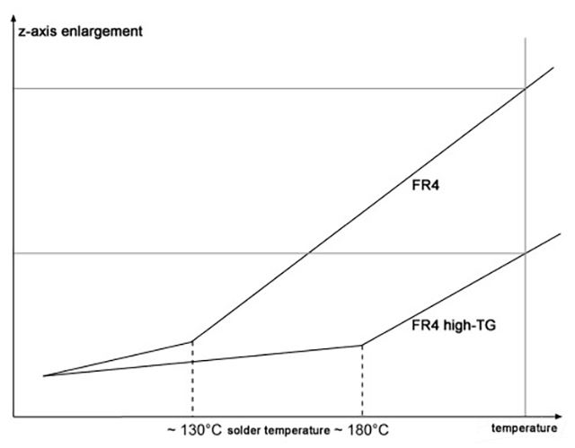
While the board doesn't turn into a liquid, entering this "rubbery" state causes the material to expand rapidly. This expansion is measured by the Coefficient of Thermal Expansion (CTE). When a board exceeds its Tg value, its thermal expansion rate can jump by 4 to 8 times, causing immense mechanical stress on the copper traces and internal structures.
Learn More: For a deeper dive into material properties, read our Guide to FR-4 PCB Material.
2. The Physics of Failure: Z-Axis CTE Mismatch
The most critical threat to a PCB during thermal cycling is the mismatch between the epoxy resin and the copper plating. While fiberglass cloth restrains expansion in the X and Y planes, the Z-axis (thickness) is largely unrestrained.
The "Z-Axis Explosion"
To understand why vias crack, look at the expansion rates:
- Copper's CTE: ≈17 ppm/°C (remains relatively constant).
- FR4's Z-Axis CTE (Below Tg, α1): ≈50-70 ppm/°C.
- FR4's Z-Axis CTE (Above Tg, α2): ≈250-300 ppm/°C.
Here is the danger zone: When the board temperature exceeds its Tg value (e.g., during reflow soldering), the resin expands at a rate (α2) that is 12 to 15 times greater than the copper barrel plating.
This mismatch exerts massive tensile stress on the Plated Through Hole (PTH). If the material spends too much time above Tg, the epoxy stretches the copper until it snaps, causing barrel cracks or corner cracks. This results in intermittent open circuits that are notoriously difficult to debug.
High Tg materials are superior because they delay this transition. By keeping the material in the low-expansion (α1) state for a wider temperature range, the total stress on your vias is significantly reduced.
3. Beyond Tg: The Hidden Metrics (Td & T288)
Top-tier engineers know that Tg is just the headline. If you are designing for high reliability, you must also look at Td and T288.
Td (Decomposition Temperature)
While the glass transition is reversible, Td is the point of no return. It is the temperature at which the PCB material physically loses 5% of its mass due to chemical decomposition.
- The Risk: Lead-free soldering profiles often peak at 240°C–260°C. If your material's Td is too low, the resin matrix begins to carbonize or oxidize during reflow. This can lead to leakage currents (CAF) or permanent structural damage.
T260 / T288 (Time to Delamination)
Measured according to IPC-TM-650 2.4.24.1, this defines how many minutes a board can withstand 260°C or 288°C before internal failure (bubbling/delamination).
- Why it matters: A standard FR4 might survive one reflow cycle. But a complex PCBA often undergoes multiple thermal cycles: Top-side reflow + Bottom-side reflow + Wave soldering + Rework. A High Tg board with robust T288 performance is essential to survive these repeated shocks without internal separation.
Related Reading: Thermal management is critical. Check out our FR4 Thermal Conductivity Overview.
4. IPC Standards: Selecting the Right Laminate
In professional fabrication, we rely on IPC-4101 (Specification for Base Materials) to categorize these laminates. Don't just ask for "Good FR4"—reference the industry standards.
| Material Class |
IPC-4101 Slash Sheet |
Tg Range |
Td (min) |
Best Application |
| Standard FR-4 |
/21 |
130°C – 140°C |
310°C |
Consumer electronics, simple prototyping, low layer count (2-4 layers). |
| Mid-Tg FR-4 |
/24 |
150°C – 160°C |
325°C |
General industrial, entry-level lead-free assembly. |
| High Tg FR-4 |
/26, /126 |
≥170°C |
340°C |
Multilayer (>6 layers), Automotive, Servers, Hi-Rel,IPC Class 3. |
You don't always need the most expensive material. However, if your design meets any of the following criteria, you should switch to High Tg.
A. The Operating Temperature Rule
A safe rule of thumb is that your maximum operating temperature should be 20°C lower than the material's Tg.
- Standard FR4 (Tg 130°C): Max operating temp ≈110°C.
- High Tg (Tg 170°C): Max operating temp ≈150°C. If your device runs hot, Standard FR4 becomes risky.
B. Lead-Free Reflow Soldering
Lead-free solders (RoHS compliance) require higher reflow temperatures, often peaking between 240°C and 260°C. While this is a short burst, standard FR4 can soften significantly, leading to the "pad cratering" or bowing mentioned earlier. For PCB Assembly Services involving complex RoHS boards, High Tg is highly recommended.
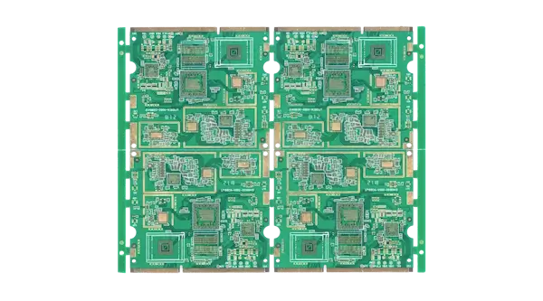
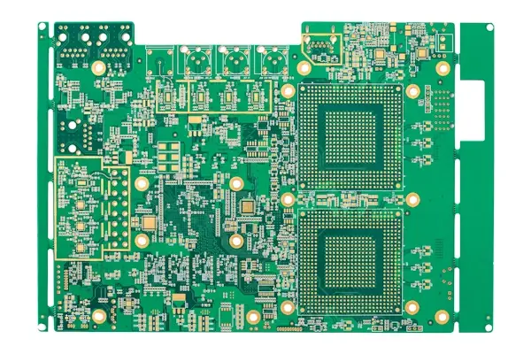
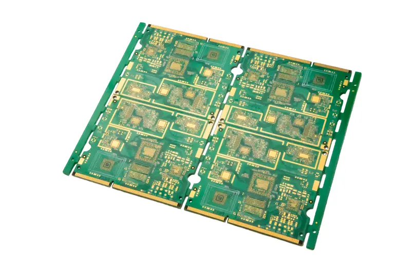
C. High Layer Counts (Multilayer PCBs)
As you add layers (6, 8, 12+), the cumulative stress of Z-axis expansion increases. The density of vias and internal traces makes the board more susceptible to thermal failure.
- Pro Tip: For boards with 10+ layers, High Tg is virtually mandatory to ensure yield.
NextPCB Capability: We specialize in IPC-4101 /126 materials that utilize inorganic fillers to further reduce Z-axis expansion and increase the Storage Modulus (measured via DMA), ensuring maximum mechanical stiffness at high temperatures. View our capabilities: High Tg PCBs | Rigid PCBs
5. When Do You Really Need High Tg?
A. The Operating Temperature Rule (Top < Tg - 20°C)
As a standard engineering practice, your maximum continuous operating temperature should be at least 20°C below the material's Tg. If your enclosure reaches 85°C, Standard FR4 (Tg ~140°C) is already at risk of structural degradation.
For designs that also carry significant current — such as power supplies, motor drives, or high‑power converters — thermal management becomes a dual concern of both substrate selection and trace heating control. Incorrect trace sizing not only increases localized temperature, but also accelerates thermal stresses that work against material reliability. To address this, designers should couple material selection with precise trace width calculation and thermal planning. For deeper guidance on this topic, see PCB Trace Width Calculation: High‑Current Design & Thermal Analysis to learn how to calculate appropriate trace widths and implement thermal mitigation strategies for high current paths (e.g., adjusting copper weight, using thermal vias, and optimizing trace geometry).
B. High Layer Counts (Multilayer PCBs)
As you add layers (6, 8, 12+), the total thickness of the board increases, and the density of vias rises. The cumulative stress of Z-axis expansion becomes much more dangerous in thick boards.
- Pro Tip: For boards with 8+ layers, High Tg is virtually mandatory to ensure manufacturing yield and via reliability.
C. Extreme Environments (Humidity & Thermal Cycling) and Rework
For aerospace or outdoor industrial applications, Tg isn't the only factor. You must also consider Dynamic Mechanical Analysis (DMA) metrics to ensure the material retains its elastic modulus under vibration while exposed to high humidity, preventing Conductive Anodic Filament (CAF) growth.
Designers often calculate thermal stress based on reflow cycles. But what about Rework? If a BGA needs to be replaced during PCB Assembly, the local area is heated strictly again. A standard FR4 board often fails during this third or fourth localized heating event, leading to pad lifting or pad cratering. High Tg materials maintain their adhesion strength (Peel Strength) much better at rework temperatures.
6. Typical Scenarios for High Tg Materials
> Automotive Electronics
Automotive environments are hostile. ECUs and sensors face extreme temperature fluctuations (thermal shock) and constant vibration. The rigidity of High Tg material is required to prevent fatigue failures over a vehicle's 10-15 year lifespan.
> Industrial Controls
Industrial PLCs often run 24/7 in non-climate-controlled enclosures. The combination of continuous internal heat generation and long service life demands materials that resist thermal aging.
> Power Supplies & Inverters
High currents generate significant heat. High Tg boards ensure that the heat generated by MOSFETs and transformers doesn't compromise the structural integrity of the PCB substrate.
Summary: Don't Let Material Selection Be Your Point of Failure
Choosing High Tg PCB material is an investment in the longevity of your product. While standard FR4 is cost-effective for simple logic, High Tg (IPC-4101 /26 or /126) is the prerequisite for multilayer, high-temp, or high-reliability IPC Class 3 applications.
Key Takeaway: If your board has dense vias, 6+ layers, requires lead-free soldering, or operates in environments above 100°C, do not compromise—choose High Tg (IPC-4101 /26).
Next Steps for Your Design
Are you unsure if your current stack-up requires High Tg material?
a. Analyze Your Design: Upload your files to our Free Online Gerber Viewer. Inspect your drill-to-copper ratios and layer density to assess expansion risks.
b. Prototype Safely: Order a PCB Prototype with NextPCB. You can select High Tg options directly in our quote tool to compare costs instantly.
c. Verify Reliability: For critical projects, utilize our Free Functional Testing service with your assembly order. We help you verify that your board can handle the heat under real-world loads.
Ready to build reliable PCBs?
Get Your Instant Quote Now
Engineering FAQ: Solving the Top 5 PCB Fabrication & Reliability Pain Points
Based on recent industry discussions and DFM (Design for Manufacturability) best practices, we've compiled solutions to the most common frustrations faced by engineers today.
1. Why does my physical PCB not match my design (missing or invalid layers)?
The Root Cause: This usually stems from corrupted Gerber/ODB++ exports, missing layer definitions in Fab Notes, or a manufacturer proceeding without a rigorous DFM/CAM review.
The Solution: Data Insight: Complete stack-up documentation and pre-export validation can reduce fabrication layer errors by over 80%.
- Pre-verify Files: Use the NextPCB Online Gerber Viewer to inspect stack-up and plating info before submittal.
- Comprehensive Fab Notes: Explicitly define the stack-up, surface finish, and solder mask requirements.
- Utilize NextPCB DFM Review: Every order undergoes a professional engineering review to catch "missing layer" errors before production starts.
2. My PCB has power-on anomalies or hard-to-trace electrical issues. What happened?
The Root Cause: Likely due to insufficient SI/PI (Signal/Power Integrity) design, poor material selection leading to thermal stress (e.g., pad cratering), or internal manufacturing defects like near-edge copper shorts.
The Solution:
- Automated DRC/DFM: Upload your Gerber to the NextPCB quote page for an instant automated rule check.
- Choose High-Reliability Materials: Opt for High Tg PCB materials to improve thermal cycle and moisture resistance.
- Post-Assembly Verification: Use NextPCB Functional Testing Services to identify electrical anomalies before the boards leave the factory.
3. How do I stop my designs from being rejected for frequent DFM issues?
The Root Cause: Common "beginner" errors include insufficient trace-to-edge spacing, drill-to-copper violations, or silk-screen-on-pad overlaps.
The Solution: Data Insight: Proper DFM checks prevent approximately 70% of common manufacturing errors and costly scrap.
- Follow Manufacturer Rules: Reference the NextPCB DFM guide to align your CAD constraints with our house capabilities.
- Early DFM Integration: Perform DFM checks during the layout phase, not just at the end.
- Engineering Coaching: Upload your design to NextPCB; our engineers provide specific feedback to prevent rework and cost overruns.
4. How can I reduce Signal Integrity (EMC/Noise) issues in high-speed designs?
The Root Cause: Poor reference plane integrity, broken return paths, or lack of impedance control leads to electromagnetic interference (EMI) and crosstalk (e.g., on CAN bus or high-speed interfaces).
The Solution:
- Impedance Control: Specify your impedance requirements during the NextPCB quoting process. We support custom stack-ups and sample verification.
- Optimized Stack-up: Ensure high-frequency signals are sandwiched between solid reference planes.
- Expert Review: Request an EMC/SI review from the NextPCB engineering team for your specific high-speed layout.
5. Why are complex/high-layer count boards more prone to reliability failure?
The Root Cause: In multilayer or HDI boards, internal stresses caused by mismatched Coefficients of Thermal Expansion (CTE) lead to Conductive Anodic Filament (CAF) growth or internal barrel cracking during thermal cycling.
The Solution:
- Select Premium Substrates: Use High Tg or filled materials (IPC-4101 /126) to minimize internal Z-axis expansion.
- Balanced Stack-up Design: Follow NextPCB's engineering advice on symmetrical stack-ups to prevent board warpage.
- Environmental Testing: Verify reliability under extreme conditions through our environmental and functional testing suites.
Ready to eliminate manufacturing risks? Whether you are building a simple PCB Prototype or a complex automotive system, NextPCB provides the material expertise and engineering support to ensure your design succeeds on the first pass.
Make the Material Switch Without Struggle
Upload & Get Professional DFM Review Today Engineer Consultation
About the Author
Lolly Zheng- Sales Account Manager at NextPCB.com
Four years of proven sales experience across electronic components and PCBA industries, with strong expertise in key account acquisition, customer relationship management, and contract negotiations. Focused on driving revenue growth through strategic client development and solution-based selling. Experienced in expanding high-value accounts, securing long-term partnerships, and consistently exceeding sales targets in competitive markets.


 NextPCB Capabilities
 PCB Assembly
 Layer Buildup
 SMD-Stencils
 PCB Design-Aid & Layout
 Mechanics
 Surface
 Quality
 Drills & Throughplating
 Factory & Certificate