
 NextPCB Capabilities
Printed Circuit Boards
NextPCB Capabilities
Printed Circuit Boards
 PCB Assembly
 Layer Buildup
 SMD-Stencils
 PCB Design-Aid & Layout
 Mechanics
 Quality
 Drills & Throughplating
 Factory & Certificate
 PCB Assembly Factory Show
Certificate
PCB Assembly Factory Show
Certificate
Support Team
Feedback:
support@nextpcb.com


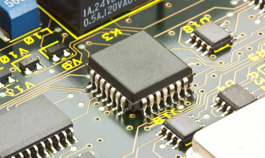
In daily life, you may encounter the abbreviation SMD in different contexts. In the medical field, SMD might refer to "Senile Macular Degeneration"; on social media, SMD can sometimes be used as a less polite abbreviation; and in management, SMD has its own strategic significance. However, when you open your sleek smartphone or observe the densely packed, sesame-sized components on a computer motherboard, SMD takes on a highly technical identity: Surface Mounted Device.
It is the absolute cornerstone of modern electronics, enabling our devices to transform from bulky equipment into the ultra-portable wonders we carry today. Today, we will delve into the meaning, full name, and crucial role of SMD in PCB manufacturing from the perspective of an experienced electronic engineer, looking at everything from component characteristics to real-world assembly costs.
The SMD full form stands for Surface Mount Device. In the electronics manufacturing field, SMD is often confused with SMT. Before diving deeper, clarifying their relationship is the critical first step:
From a hardware engineering perspective, an SMD is an electronic component specifically engineered for direct mounting onto the surface of PCB pads. It fundamentally disrupts traditional Through-Hole Technology (THT):
As an engineer who's spent years walking the factory floor and analyzing Gerber files, I always tell hardware startups: The industry's move to SMD wasn't about aesthetics. It was a mandatory evolution driven by efficiency, signal integrity, and scalable production costs.
Twenty years ago, a standard resistor was about half the size of a matchstick. Today, commonly used 0201 packages (0.6mm x 0.3mm) and 01005 packages are almost invisible to the naked eye. As we move through 2026, advanced consumer electronics are increasingly adopting even smaller 008004 packages. This exponential leap in size reduction allows designers to pack thousands of functional units onto a PCBA the size of a smartwatch dial.
Because SMD components have virtually no leads, the electrical pathways are incredibly short. This results in:
Understanding SMD specifications is just the starting point; translating that into high-yield, low cost PCB production runs is where real engineering happens. Below are the core steps in the PCB assembly line and practical Design for Manufacturing (DFM) tips to avoid costly delays.
In your EDA software (like Altium, KiCad, or Eagle), the footprint design directly dictates the final soldering quality. A poorly designed footprint will cause defects on the assembly line, regardless of how good the machines are.
Ask any seasoned SMT technician, and they will tell you that over 70% of SMD soldering defects originate at the solder paste printing stage.
This is the heartbeat of quick turn PCB assembly. Automated pick-and-place machines shoot components onto the board at speeds exceeding 100,000 Components Per Hour (CPH).
To help you navigate Bills of Materials (BOMs), we categorize common SMDs into the following major families:
| Type | Representative Components | Common Packages | Engineer Comments & DFM Notes |
|---|---|---|---|
| Passive Components | Resistors, Capacitors, Inductors | 0201, 0402, 0603, 0805, 1206 | The smaller they get (like 01005), the tighter the layout, but manual rework becomes impossible without specialized hot-air stations. |
| Discrete Semiconductors | Diodes, Transistors, Rectifiers | SOT-23, SOT-89, SOD-123, SMA | Evergreen choices for power conversion. Pay close attention to polarity markings during footprint creation to avoid reversed assembly. |
| Integrated Circuits (IC) | Microcontrollers, DSPs, Memory | SOIC, QFP, QFN, BGA | The exposed center pad on the bottom of a QFN is critical for heat dissipation; ensure your footprint includes thermal vias to the ground plane. |
| Electromechanical | Tactile Buttons, USB/Type-C Connectors | SMD Switches, SMT Headers | Mechanical stress is the enemy here. SMT connectors often utilize THT positioning pegs (Through-Hole Reflow) to reinforce the mechanical strength against unplugging forces. |
In high-grade PCB manufacturing, placing the component is only half the battle. After the SMDs pass through the multi-zone reflow oven, they must undergo strict quality control to guarantee reliability:
> Recommend reading: How does NextPCB conduct quality control?
If someone asks you, "What is the definition of SMD?", the dictionary answer is straightforward. However, the true meaning changes depending on your role in the hardware lifecycle:
SMD is not just a type of component package; it is the physical foundation of modern electronics manufacturing. Mastering its principles is a required core competence for anyone bringing hardware to market.
> Recommend reading: SMT Meaning in Medical, Automotive, Industrial & Consumer Electronics
Understanding SMD package sizes is one of the most practical skills a PCB designer can develop. The package you choose directly determines pad geometry, stencil aperture, pick-and-place requirements, and ultimately your assembly yield — long before a single solder joint is formed. This section breaks down the standard dimensions across every major SMD package family so you can cross-reference your BOM and layout decisions with confidence.
Passive SMD components use a four-digit imperial naming code that directly encodes body length and width in hundredths of an inch. A 0402, for example, measures 0.04 in × 0.02 in — or 1.0 mm × 0.5 mm in metric terms.
>> Passive Component Symbols Visual Reference
| Imperial Code | Metric Equivalent | Body Size (L × W, mm) | Typical Power Rating | Common Use |
|---|---|---|---|---|
| 01005 | 0402M | 0.4 × 0.2 | 1/32 W | Ultra-miniature consumer devices |
| 0201 | 0603M | 0.6 × 0.3 | 1/20 W | Wearables, RF front-ends |
| 0402 | 1005M | 1.0 × 0.5 | 1/16 W | Mobile, high-density PCBs |
| 0603 | 1608M | 1.6 × 0.8 | 1/10 W | General purpose; easiest to hand-solder |
| 0805 | 2012M | 2.0 × 1.25 | 1/8 W | Power supplies, industrial boards |
| 1206 | 3216M | 3.2 × 1.6 | 1/4 W | Higher voltage/current passives |
| 1210 | 3225M | 3.2 × 2.5 | 1/2 W | High-capacitance MLCCs |
| 2010 | 5025M | 5.0 × 2.5 | 3/4 W | Current sense resistors |
| 2512 | 6332M | 6.3 × 3.2 | 1 W | High-power shunt resistors |
Quick rule of thumb: For prototyping or hand-rework, 0603 is the practical minimum. In high-volume automated production, 0402 is the industry workhorse. Reserve 0201 and smaller for space-constrained designs where your CM has verified SMT line capability — not all lines reliably handle 01005.
Small-signal semiconductors are housed in the SOT (Small Outline Transistor) and SOD (Small Outline Diode) package families. Body height and pad geometry vary considerably across the range, which matters for thermal calculations and reflow profile selection.
| Package | Pins | Body Size (L × W × H, mm) | Max Current | Typical Application |
|---|---|---|---|---|
| SOT-23 | 3 | 2.9 × 1.3 × 1.0 | — | BJTs, small-signal MOSFETs |
| SOT-23-5 | 5 | 2.9 × 1.6 × 1.0 | — | Op-amps, LDOs |
| SOT-89 | 3 | 4.5 × 2.5 × 1.5 | ~1 A | Medium-power transistors |
| SOT-223 | 4 | 6.7 × 3.6 × 1.8 | ~2 A | Voltage regulators |
| SOT-252 (DPAK) | 3 | 9.9 × 6.5 × 2.3 | ~10 A | Power MOSFETs, linear regulators |
| SOT-263 (D2PAK) | 7 | 10.3 × 8.1 × 2.3 | ~30 A | High-current switching devices |
| SOD-123 | 2 | 2.8 × 1.8 × 1.0 | 1 A | Rectifier diodes |
| SOD-323 | 2 | 1.7 × 1.25 × 0.95 | 0.2 A | High-speed switching diodes |
| SMA (DO-214AC) | 2 | 4.4 × 2.7 × 2.1 | 1 A | TVS, Schottky diodes |
| SMB (DO-214AA) | 2 | 5.0 × 3.6 × 2.2 | 2 A | Power rectifiers |
| SMC (DO-214AB) | 2 | 7.9 × 5.9 × 2.4 | 5 A | High-power protection diodes |
Engineering Tip: When upgrading from SOT-23 to SOT-223 for thermal relief, verify that your PCB layout provides adequate copper pour on the tab. Thermal resistance can drop from ~150°C/W to ~60°C/W — but only if the pad is properly connected to a ground plane.
Integrated circuits span the widest range of SMD package geometries — from a 2×2 mm QFN-8 to a 35×35 mm FC-BGA. The package family you select cascades into routing layer count, via strategy, BOM cost, and long-term repairability.
SOIC / SOP — Gull-Wing Leaded Packages
The workhorse of analog and digital ICs, leaded SOP packages remain popular for designs where hand-rework accessibility is a priority.
| Package | Pitch (mm) | Pins | Body Width (mm) | Notes |
|---|---|---|---|---|
| SOIC-8 | 1.27 | 8 | 3.9 | Most common analog IC footprint |
| SOIC-14 / 16 | 1.27 | 14–16 | 3.9 | Logic gates, interface ICs |
| TSSOP-8 | 0.65 | 8 | 3.0 | Thin, fine-pitch variant |
| SSOP-16 | 0.635 | 16 | 5.3 | Mid-density digital ICs |
| MSOP-8 | 0.65 | 8 | 3.0 | Miniature precision analog |
QFP — Quad Flat Pack
QFP packages are the standard choice for MCUs and DSPs requiring high I/O counts with visible, inspectable leads.
| Package | Pitch (mm) | Pins | Body Size (mm) | Typical Use |
|---|---|---|---|---|
| LQFP-32 | 0.8 | 32 | 7 × 7 | Entry-level MCUs |
| LQFP-48 | 0.5 | 48 | 7 × 7 | Mid-range MCUs |
| LQFP-64 | 0.5 | 64 | 10 × 10 | ARM Cortex-M class |
| LQFP-100 | 0.5 | 100 | 14 × 14 | High-peripheral-count MCUs |
| LQFP-144 | 0.5 | 144 | 20 × 20 | FPGA, high-end MCUs |
Engineering Tip: QFP packages at 0.5 mm pitch require laser-cut stencils with ~10–15% aperture reduction and mandatory SPI inspection after paste printing. At 0.4 mm pitch, optical pre-alignment on the pick-and-place becomes non-negotiable — confirm your CM’s capability before finalizing the package choice.
QFN — Quad Flat No-Lead
QFN packages deliver smaller footprints and lower parasitic inductance compared to QFP, making them the preferred choice for RF, power management, and high-frequency signal processing.
| Package | Pins | Body Size (mm) | Pitch (mm) |
|---|---|---|---|
| QFN-8 | 8 | 2 × 2 | 0.5 |
| QFN-16 | 16 | 3 × 3 | 0.5 |
| QFN-32 | 32 | 5 × 5 | 0.5 |
| QFN-48 | 48 | 6 × 6 | 0.5 |
| QFN-64 | 64 | 8 × 8 | 0.5 |
The exposed thermal pad on the underside is a key thermal advantage — but it must be connected to inner copper planes via via-in-pad stitching. Without this, the thermal resistance values in the datasheet are simply not achievable in a real assembly.
BGA — Ball Grid Array
BGA packages trade visual inspectability for the highest possible I/O density and electrical performance, making them the mandatory choice for processors, FPGAs, and high-speed memory.
| Package Variant | Ball Pitch (mm) | Application |
|---|---|---|
| PBGA | 1.0 – 1.27 | Processors, FPGAs |
| FBGA | 0.8 | DDR memory |
| μBGA / CSP | 0.5 | Mobile SoCs |
| WLCSP | 0.4 | Smartphone PMICs |
| FC-BGA | 1.0 | CPUs, GPUs |
Because BGA solder balls are hidden beneath the package body, X-ray inspection is non-negotiable after placement — an AOI pass alone cannot verify joint integrity on any BGA variant.
The same physical passive package carries two different names depending on the supply chain your distributor uses. Imperial codes are standard in North America; metric codes dominate Japanese and Korean suppliers. Both refer to identical components.
| Imperial | Metric | L (mm) | W (mm) |
|---|---|---|---|
| 0201 | 0603M | 0.6 | 0.3 |
| 0402 | 1005M | 1.0 | 0.5 |
| 0603 | 1608M | 1.6 | 0.8 |
| 0805 | 2012M | 2.0 | 1.25 |
| 1206 | 3216M | 3.2 | 1.6 |
| 1210 | 3225M | 3.2 | 2.5 |
| 2512 | 6332M | 6.3 | 3.2 |
Engineering Tip: Normalize your BOM to a single naming convention before submitting to your CM. Mixed imperial/metric codes on the same BOM are among the most common causes of kitting errors at the component warehouse — a preventable mistake that delays production runs.
For pad geometry and courtyard dimensions behind these packages, the governing reference is IPC-7351B, which defines land pattern standards for all surface mount component families.
The shift from through-hole (THT) to surface mount technology wasn’t a stylistic choice — it was an engineering mandate driven by density, speed, and cost. That said, through-hole components haven’t disappeared, and for good reason. Knowing exactly where each technology wins is what separates a good layout decision from an expensive one.
| Criteria | SMD | Through-Hole (THT) |
|---|---|---|
| Component size | Significantly smaller; 0402 is ~10× smaller than a comparable DIP package | Larger body and lead footprint |
| Board density | Both sides of the PCB usable; supports high-density routing | Single-side mounting only; drill holes consume routing space on all layers |
| Assembly speed | Pick-and-place at 10,000–100,000+ CPH; fully automated | Wave soldering or hand insertion; slower throughput |
| Assembly cost (volume) | Lower at scale; minimal human labor | Higher; manual placement or selective soldering adds cost |
| Prototype / hand assembly | Requires skill; fine-pitch packages (<0.5 mm) are difficult without tools | Beginner-friendly; straightforward hand-soldering |
| Electrical performance | Lower parasitic inductance and capacitance; better high-frequency behavior | Longer lead lengths introduce parasitic inductance; less suitable above ~100 MHz |
| Thermal dissipation | Limited by small pad area; power packages use exposed pads and via-in-pad | Lead frame and bulk body conduct heat more effectively; easier to heatsink |
| Mechanical strength | Joints are on the surface only; vulnerable to vibration and mechanical shock | Leads pass through the board; inherently stronger mechanical bond |
| Reworkability | Hot-air or IR rework station required; BGA rework is specialized | Desoldering wick or vacuum pump; straightforward for most skill levels |
| Component availability | Broadest selection; most new ICs are SMD-only | Shrinking catalog; legacy and high-power components still common |
| PCB cost impact | No drill holes for component leads; reduces layer stackup complexity | Via drilling adds per-hole cost; high-density THT boards cost more to fabricate |
| Inspection | AOI covers most packages; BGA/QFN require X-ray | Visual inspection sufficient for most joints; X-ray rarely needed |
| Reliability (vibration) | Lower without underfill; BGA particularly vulnerable to flex | Superior mechanical anchoring; preferred in aerospace and automotive |
| Best fit | Consumer electronics, mobile, RF, high-density digital | Power supplies, connectors, high-voltage, harsh-environment applications |
Engineering Tip: In practice, most production boards are mixed-technology — SMD for ICs and passive components, THT retained for high-current connectors, electrolytic capacitors, and components subject to mechanical stress. Designing for mixed assembly requires careful process sequencing: SMD reflow first, THT wave or selective soldering second.
Even a well-designed PCB can fail at the assembly stage if solder joint formation goes wrong. The two most prevalent SMD defects — tombstoning and solder bridging — account for a disproportionate share of yield losses on SMT lines. Understanding the root cause of each is the fastest path to eliminating them.
Tombstoning (also called the “Manhattan effect” or “drawbridge effect”) occurs when one end of a passive component lifts off its pad during reflow, leaving the component standing vertically on one terminal. The result is an open circuit on the lifted end and a cold or shifted joint on the other.
Root cause: The two pads on a passive component reach liquidus temperature at different moments during reflow. The pad that melts first exerts surface tension on that end of the component; if the opposing pad hasn’t yet melted to provide a counterbalancing pull, the component is dragged upright.
Contributing factors:
Prevention strategies:
| Corrective Action | How It Helps |
|---|---|
| Balance pad copper geometry | Equalizes heat absorption on both ends |
| Avoid placing large copper pours adjacent to one pad only | Reduces thermal asymmetry |
| Use symmetric stencil apertures | Ensures equal paste volume per pad |
| Increase reflow ramp rate (within profile limits) | Minimizes time at temperature delta between pads |
| Orient components perpendicular to conveyor direction | Both pads enter the reflow zone simultaneously |
| Apply thermal relief on ground-connected pads | Slows heat absorption on the grounded side to match the ungrounded side |
A solder bridge is an unintended conductive connection between two adjacent pads or leads. On fine-pitch ICs, a single bridge can short power to ground or corrupt a data bus — and on densely populated boards, bridges are notoriously difficult to locate by AOI alone.
Root cause: Excess solder material flows beyond pad boundaries and contacts an adjacent conductor. This can occur during paste printing, reflow, or wave soldering.
Contributing factors:
Prevention strategies:
| Corrective Action | How It Helps |
|---|---|
| Reduce stencil aperture by 10–20% for fine-pitch pads | Limits paste volume to what the pad can contain |
| Verify solder mask web width ≥ 75 μm between pads | Provides a physical barrier against solder flow |
| Use Type 4 or Type 5 paste for pitches ≤ 0.5 mm | Smaller particle size enables finer aperture printing without clogging |
| Run SPI (Solder Paste Inspection) after every print cycle | Catches excess or misaligned paste before reflow |
| Tighten pick-and-place Cpk on fine-pitch components | Prevents misalignment-induced bridging |
| Optimize reflow peak temperature | Overly high peak temperatures reduce paste viscosity and promote spread |
Engineering Tip: On boards with both coarse-pitch through-hole and fine-pitch SMD components, wave soldering the THT stage after SMD reflow is the standard process — but wave solder flux and turbulence can wick into QFP and SOIC pads and cause bridges on the SMD side. Apply selective solder mask or peel-away tape to SMD areas before any wave exposure to prevent this.
For context, world-class SMT lines targeting IPC Class 2 (standard commercial) typically achieve:
| Defect Type | Acceptable Rate (IPC Class 2) | World-Class Target |
|---|---|---|
| Tombstoning | < 50 DPMO | < 10 DPMO |
| Solder bridging | < 100 DPMO | < 20 DPMO |
| Insufficient solder | < 200 DPMO | < 50 DPMO |
| Component misalignment | < 100 DPMO | < 15 DPMO |
DPMO = Defects Per Million Opportunities. Achieving world-class targets requires closed-loop SPI data feeding back into paste printer parameter adjustments in real time — a capability available on modern inline inspection systems but often underutilized on older SMT lines.
Transitioning from a prototype design to a fully populated PCBA requires a manufacturing partner who deeply understands SMD tolerances and SMT processes. At NextPCB, we specialize in high-reliability turnkey PCB solutions.
Whether you need a quick turn PCB prototype using 0201 passives or a high-volume production run with complex BGAs, our state-of-the-art facilities ensure your designs are assembled with aerospace-level precision. We handle everything from PCB fabrication and component sourcing to final assembly and X-Ray inspection, saving you time and reducing your overall project costs. Stop worrying about tombstoning and solder voids—let the experts handle your next PCBA project.
> Read More: Turnkey PCBA Component Sourcing: Questions You Must Ask Before You Order
A: In the electronics industry, SMD stands for Surface Mounted Device. It refers to electronic components (like resistors, capacitors, diodes, and microchips) designed with flat contacts or short leads to be soldered directly onto the surface of a Printed Circuit Board (PCB), eliminating the need for drilling holes for component leads.
A: While often used interchangeably by beginners, they have distinct technical meanings:
1. SMD (Surface Mounted Device) refers to the physical hardware component itself (the part you place on the board).
2. SMT (Surface Mount Technology) refers to the manufacturing process, machinery, and techniques used to place and solder those SMDs onto the bare circuit board.
A: SMD components are heavily preferred in modern PCBA because they allow for extreme miniaturization and higher component density. Because they do not require drilled holes, boards can be smaller and cheaper to manufacture. Furthermore, SMDs can be placed by robots at massive speeds (reducing assembly costs) and possess better electrical characteristics for high-frequency signal routing.
A: Common SMD packages in PCB manufacturing include:
- Passives: Imperial sizes like 0402, 0603, 0805, and 1206 (for resistors and capacitors).
- Transistors/Diodes: SOT-23, SOD-323.
- Integrated Circuits: SOIC (Small Outline IC), QFP (Quad Flat Package), QFN (Quad Flat No-leads), and BGA (Ball Grid Array).
A: Yes, but it requires practice and the right tools. While large SMDs like 1206 resistors or SOIC chips can be hand-soldered with a fine-tipped soldering iron and flux, micro-components (like 0201) or leadless packages (like QFN and BGA) require a hot air rework station, solder paste, and a microscope to properly melt the solder without bridging.
A: SMD component sizes depend on component type. For passive components (resistors, capacitors, inductors), the most common package sizes are:
For transistors and diodes, SOT-23 (2.9 × 1.3 mm) and SOT-223 (6.7 × 3.6 mm) are the go-to packages. For ICs, SOIC-8 is the workhorse for analog devices, QFN packages run from 2×2 mm to 8×8 mm, and BGA variants cover everything from compact mobile SoCs to large FPGA substrates.
As a rule of thumb: 0603 for prototyping, 0402 for production, and 0201 or below only when board space is the hard constraint.
Still, need help? Contact Us: support@nextpcb.com
Need a PCB or PCBA quote? Quote now


 Surface

