
 NextPCB Capabilities
Printed Circuit Boards
NextPCB Capabilities
Printed Circuit Boards
 PCB Assembly
 Layer Buildup
 SMD-Stencils
 PCB Design-Aid & Layout
 Mechanics
 Quality
 Drills & Throughplating
 Factory & Certificate
 PCB Assembly Factory Show
Certificate
PCB Assembly Factory Show
Certificate

Support Team
Feedback:
support@nextpcb.com


In the spotlight of the electronics industry, attention often focuses on smartphones, foldable screens, or the latest AI servers. However, behind these flashy consumer electronics is a silent giant that supports global manufacturing operations, maintains the stability of energy networks, and drives automated production lines—Industrial Control PCBs.
As global manufacturing transitions to "Industry 4.0" and smart manufacturing, Industrial Control PCBs are evolving from traditional "electronic carriers" to core neural systems that support high computing power, high power, and high reliability.
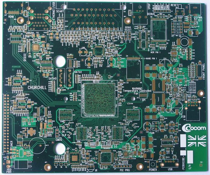
10 Layers Industrial Control PCB made by NextPCB
Industrial Control PCB refers to printed circuit boards specifically used in the field of industrial control. Unlike the circuit boards in our smartphones, Industrial Control PCBs do not pursue extreme thinness (except for some handheld industrial terminals) but instead aim for maximum stability.
Imagine: a smartphone may be replaced every two years and typically operates in a comfortable room temperature. In contrast, a PCB for an industrial servo drive may need to function continuously without downtime in a factory environment filled with oil, dust, high temperatures (over 60°C), high vibration, and even strong electromagnetic interference for 10 to 15 years.
Thus, from an industry perspective, the core definition of Industrial Control PCB is an electrical interconnection platform that achieves long life and high reliability in harsh environments.
This extreme industrial demand defines the core challenges faced by industrial control engineers: while engineers in consumer electronics often negotiate between space and cost, their primary adversaries in the industrial control field are time and environment.
Designing a board that can operate 24/7 is straightforward, but designing a PCB that can continuously run without failure for 10 years (MTBF > 50,000 hours) under conditions of 60°C, strong electromagnetic interference, and sustained vibration requires profound engineering expertise.
This necessitates that industrial control engineers focus on solving three core issues in their designs:
Consequently, the design of Industrial Control PCBs is no longer a simple routing task but an engineering art that transforms theoretical knowledge into extreme industrial reliability.
The foundation of Industrial Control PCBs must be stable; otherwise, even the best routing cannot guarantee long-term reliability. Therefore, industrial control engineers must far exceed consumer electronics standards in terms of material selection and standard definitions.
When industrial equipment goes offline, losses can amount to thousands of dollars per minute, necessitating that PCBs possess extraordinarily high durability. This is directly reflected in the strict selection of thermal properties for the substrates.
Raising the Glass Transition Temperature (Tg):
Importance of Thermal Decomposition Temperature (Td):
In industrial power sources, frequency converters, and servo drives, PCBs may need to carry currents ranging from several dozen to hundreds of amperes.
The management of Industrial Control PCBs' extended lifecycle requires adherence to the industry's highest standards to ensure manufacturability and quality.
1.3.1 Selection of IPC Standards: In design notes, it is essential to explicitly state the acceptance standards:
1.3.2 Lifecycle Commitment: Industrial equipment undergoes lengthy certification processes, and once a design is finalized, clients do not wish for arbitrary changes. Industrial control PCB manufacturers must ensure the long-term stability of their supply chains.
Attention must be paid to the reliability at the physical level (Design for Reliability), primarily addressing issues of heat, high voltage, and vibration.
Industrial control cabinets are typically sealed and fanless, with the PCB itself acting as a heat sink.
The industrial control environment is filled with high voltages (220V/380V AC). Layout engineers must always refer to IEC 60950-1 or IEC 62368-1 standards.
For equipment installed on robotic arms or vibration tables:
This aspect distinguishes junior engineers from seasoned experts. How can one ensure that an MCU does not reset and that ADC sampling remains stable next to a robot performing arc welding?
In high-temperature, high-humidity environments with voltage bias, copper filaments can grow between the glass fiber bundles in the PCB, leading to insulation failure.
Industrial control boards typically involve multiple grounds: Protective Earth (PE), Chassis Ground, Digital Ground (GND_D), Analog Ground (GND_A), and Power Ground (GND_P).
The final line of defense.
Industrial Control PCBs are widely distributed across various levels of industrial automation systems:
1. Control Layer: PLC and Industrial PCs (IPC)
This is the core of automation. PCBs are often multilayer (6-16 layers), integrating high-performance processors, memory, and complex communication interfaces. They demand high signal integrity and low latency.
2. Drive Layer: Inverters and Servo Systems
Responsible for driving motors. PCBs here emphasize thermal performance (often using metal core PCBs or thick copper boards) and high-voltage insulation capabilities.
3. Execution and Sensing Layer: Sensors and Instrumentation
Micro PCBs inside pressure, temperature, and flow sensors require high precision and environmental resistance.
4. Robotics and Mechanical Arms
With the rise of collaborative robots, there is a demand for PCBs to evolve towards miniaturization and Rigid-Flex designs while maintaining high reliability to accommodate the flexible movements of robotic joints.
Looking ahead to 2025 and beyond, the industrial control PCB market is undergoing profound transformation:
1. High Frequency and Speed Driven by Industrial IoT (IIoT)
With the proliferation of 5G and Time-Sensitive Networking (TSN), the data transmission volume within factories is surging. Future industrial control PCBs must not only be robust but also fast. This indicates that high-frequency materials (such as PTFE) will increasingly enter the industrial control sector.
2. Integration of Automation and AI
Edge computing is making its way into factory floors. Industrial control boards equipped with AI chips will become more commonplace, driving the application of HDI (High-Density Interconnect) technology in industrial PCBs—integrating more powerful computing capabilities within limited space.
3. Regional Supply Chain Reconstruction
Geopolitical factors are prompting Western countries to promote the return of manufacturing (such as Germany’s industrial strategy). This presents both challenges and significant opportunities for PCB manufacturers that have strong delivery capabilities and comply with rigorous certifications (like UL and IEC).
1. Manufacturing Capabilities and Process Benchmarking
First, the supplier must possess the technical expertise to handle the specialized processes mentioned above:
2. Stringent Quality Certification and Acceptance Systems
The core of industrial products is "traceability." A top-tier manufacturer should satisfy:
3. PCBA Assembly and Protection Processes
Industrial PCB assembly is not just soldering, but system hardening:
4. Vertically Integrated Turnkey Services
For industrial control clients, choosing a Turnkey Solution provider (PCB Manufacturing + Component Sourcing + SMT Assembly+Final Testing) significantly mitigates risk. This prevents finger-pointing between the board shop and the assembly house when defects occur (such as cold solder joints caused by PCB pad oxidation or high thermal mass), allowing for a more efficient closed-loop resolution of quality issues.
Check NextPCB Quality Control Process View NextPCB's Certifications
Industrial Control PCBs are the foundational platform for achieving long-term stable operations in modern industrial systems. Unlike consumer products that prioritize rapid iteration, they focus on providing continuous, high-reliability electrical interconnections in extremely harsh environments. As global industry transitions toward smarter and greener solutions, the strategic value of this core technology is being re-evaluated and redefined.
The challenges in designing Industrial Control PCBs do not lie in the use of high-end chips but in the precise control of boundary conditions—engineering is, in essence, an art of trade-offs.
As engineers, when routing a trace, one must consider more than just the schematic:
For investors and practitioners, focusing on Industrial Control PCB companies with advanced HDI capabilities, thick copper technology reserves, and global delivery capabilities will be crucial to grasping the pulse of future industries. Only by deeply understanding and addressing these extreme boundary conditions can we truly support the reliable operation of the future industrial landscape.
Order Components Online - Free Shipping
You may also be interest in....
> PCB Assembly - The Most Comprehensive Guide | NextPCB
> NextPCB Quality Control Process
Industrial control PCBs are engineered for extreme reliability, extended operational lifespans, and high-performance stability. Key differences include thicker copper weights for higher current loads, high-Tg (Glass Transition Temperature) substrates to withstand heat, rigorous conformal coatings for environmental protection, and adherence to IPC Class 3 standards for mission-critical reliability.
For high-heat or extreme thermal cycling environments, we recommend high-Tg FR-4 or Metal Core PCBs (MCPCB/Aluminum-clad boards). High-Tg materials prevent warping under thermal stress, while MCPCBs offer superior thermal conductivity to dissipate heat from critical components.
Key strategies include applying professional-grade conformal coatings, using potting compounds to encapsulate the assembly for complete physical sealing, and utilizing IP67/IP68-rated industrial connectors to prevent fluid ingress.
To minimize Electromagnetic Interference (EMI), designers should implement multi-layer stack-ups with dedicated ground planes, physically isolate sensitive analog circuitry from high-noise power sections, and use controlled impedance differential pair routing.
Thermal stress is a leading cause of solder joint cracking and component degradation in heavy-load applications. Proper heat source distribution and the use of thermal vias/heat sinks are essential to increase the Mean Time Between Failures (MTBF) of the system.
Still, need help? Contact Us: support@nextpcb.com
Need a PCB or PCBA quote? Quote now




